High Speed Level Shift Circuit with Reduced Skew and Method for Level Shifting

Inactive Publication Date: 2007-07-19
CYPRESS SEMICON CORP
View PDF8 Cites 23 Cited by
  • Summary
  • Abstract
  • Description
  • Claims
  • Application Information

AI Technical Summary

Benefits of technology

[0025] Preferably, the at least one level shift circuit may also include a feedback transistor, a pulse generator and a latch. As noted above, the feedback transistor may be coupled for reducing a fall delay associated with the level shift circuit by receiving a short duration pulse, which is adapted to deactivate one of the pull-up transistors faster. The pulse gene

Problems solved by technology

However, reducing the feature size also reduces the transistor's gate oxide voltage tolerance, or the maximum voltage level that may be supplied to the transistor gate without causing gate oxide degradation or breakdown.
Performance issues arise when the gate oxide begins to degrade, with circuit failure occurring when the gate oxide reaches breakdown.
This is an important challenge

Method used


Image

  • High Speed Level Shift Circuit with Reduced Skew and Method for Level Shifting
  • High Speed Level Shift Circuit with Reduced Skew and Method for Level Shifting
  • High Speed Level Shift Circuit with Reduced Skew and Method for Level Shifting

Examples


Embodiment Construction

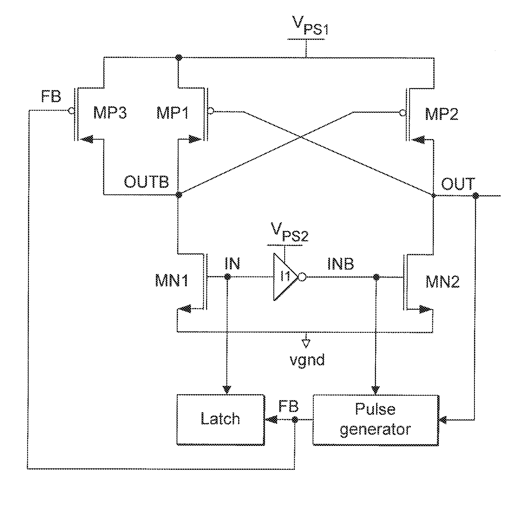
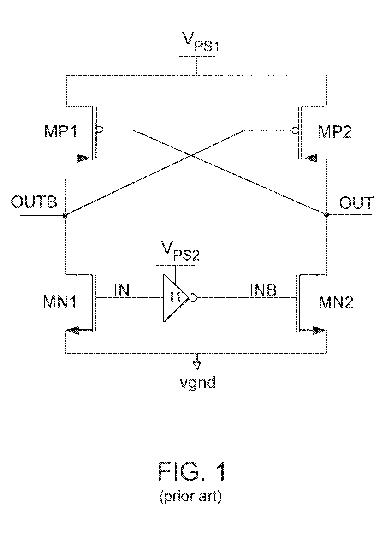
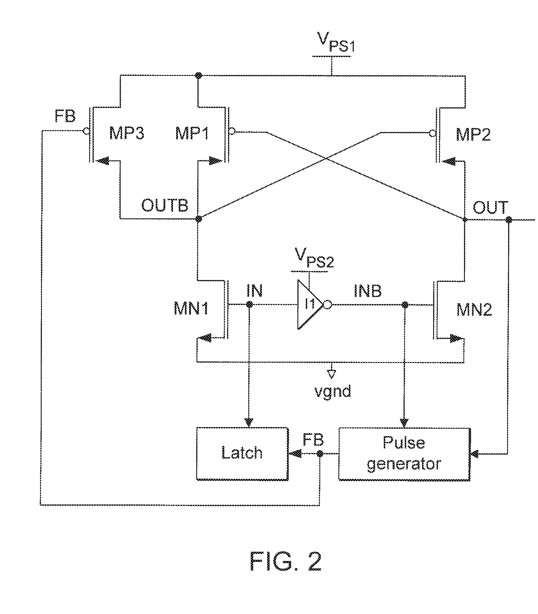
[0034]FIG. 2 shows a circuit diagram of an improved level shift circuit, according to one embodiment of the invention. As described in more detail below, the improved level shift circuit is configured to operate at very high speeds and with reduced skew. Compared to the conventional solution shown in FIG. 1, the improved level shift circuit shown in FIG. 2 may, in some cases, reduce rise / fall propagation delays from about 1.65 nanoseconds (ns) to about 400 picoseconds (ps) over a voltage range of about 1.35V to about 3.6V. The improved level shift circuit may also reduce skew between rise and fall transitions from about 540 ps (worst case) to about 200 ps (worst case), when compared to the conventional solution.

[0035] Of course, one skilled in the art would recognize that these values may be dependent on a variety of process and design factors including, but not limited to, the particular process technology used, I / O and core voltage signal level range, operating frequency, and the...


PUM


Abstract

An improved level shift circuit and method for level shifting is disclosed herein. In general, the improved level shift circuit adds a pulse generator, a feedback transistor and a latch to a conventional cross-coupled level shift circuit configuration. The pulse generator and feedback transistor are configured for reducing a fall delay associated with the level shift circuit. For example, the pulse generator is coupled for supplying a short duration feedback pulse to the feedback transistor during a first time period when input and output signals of the level shift circuit transition to a LOW state. The feedback pulse reduces the fall delay by increasing the speed with which the output signal is pulled LOW. The latch is coupled for preventing the feedback signal from floating when at least one of the input and output signals is HIGH. An integrated circuit comprising at least one level shift circuit is also contemplated herein.

Description

PRIORITY CLAIM [0001] This application claims priority to Indian Application No. 72 / CHE / 2006 filed Jan. 17, 2006 and U.S. Provisional Application No. 60 / 743,755 filed Mar. 24, 2006.BACKGROUND OF THE INVENTION [0002] 1. Field of the Invention [0003] This invention relates generally to integrated circuits, and in particular, to a high speed level shift circuit with reduced skew. More specifically, the invention provides an improved level shift circuit configured for reducing rise and fall propagation delays, as well as the amount of mismatch (i.e., skew) between such delays. [0004] 2. Description of the Related Art [0005] The following descriptions and examples are given as background only. [0006] Some I / O standards may require an integrated circuit (IC) to interface with external voltages that are significantly higher than the internal voltages used within the IC. For example, advancements in integrated circuit process technology have allowed the feature size of a transistor to be re...

Claims


Application Information

Patent Timeline
IPC IPC(8): H03K19/0175
CPCH03K19/018528
Inventor PANJWANI, GEETAJANDHYALA, APARNAMATTOS, DERWIN M.
Owner CYPRESS SEMICON CORP
Why Eureka
Try Eureka