Thin ic tag and method for manufacturing same

a thin ic tag and manufacturing method technology, applied in the direction of collapsible/retractable loop antenna, burglar alarm mechanical actuation, instruments, etc., can solve the problems of increasing the number of steps, increasing the cost of manufacturing the thin ic tag, and increasing the manufacturing cost, so as to achieve the effect of not increasing the manufacturing cost and mounting easy

Inactive Publication Date: 2007-07-19
ORMON CORP
View PDF3 Cites 26 Cited by
  • Summary
  • Abstract
  • Description
  • Claims
  • Application Information

AI Technical Summary

Benefits of technology

[0021] According to the foregoing method, the thin IC tag having the foregoing arrangement can be manufactured, but the number of manufacturing steps and the manufacturing cost are not increased. Further, the electronic part and the like are mounted easily.

Problems solved by technology

This raises such a problem that the number of manufacturing steps and the cost of manufacturing are increased.
This causes increase of the number of steps and the cost in manufacturing the thin IC tag.
This raises such a problem that mass productivity is reduced.

Method used


Image

  • Thin ic tag and method for manufacturing same
  • Thin ic tag and method for manufacturing same
  • Thin ic tag and method for manufacturing same

Examples


embodiment 1

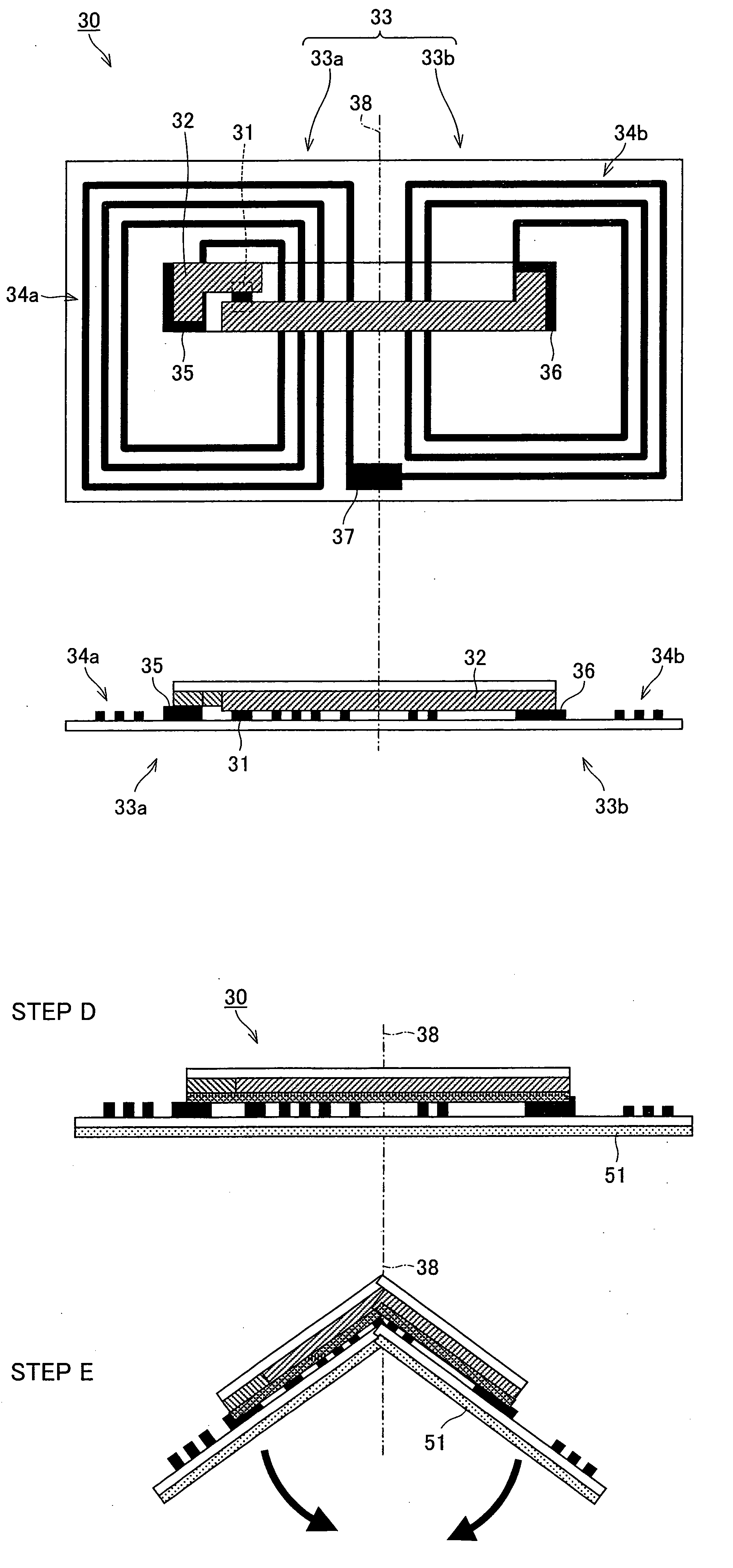
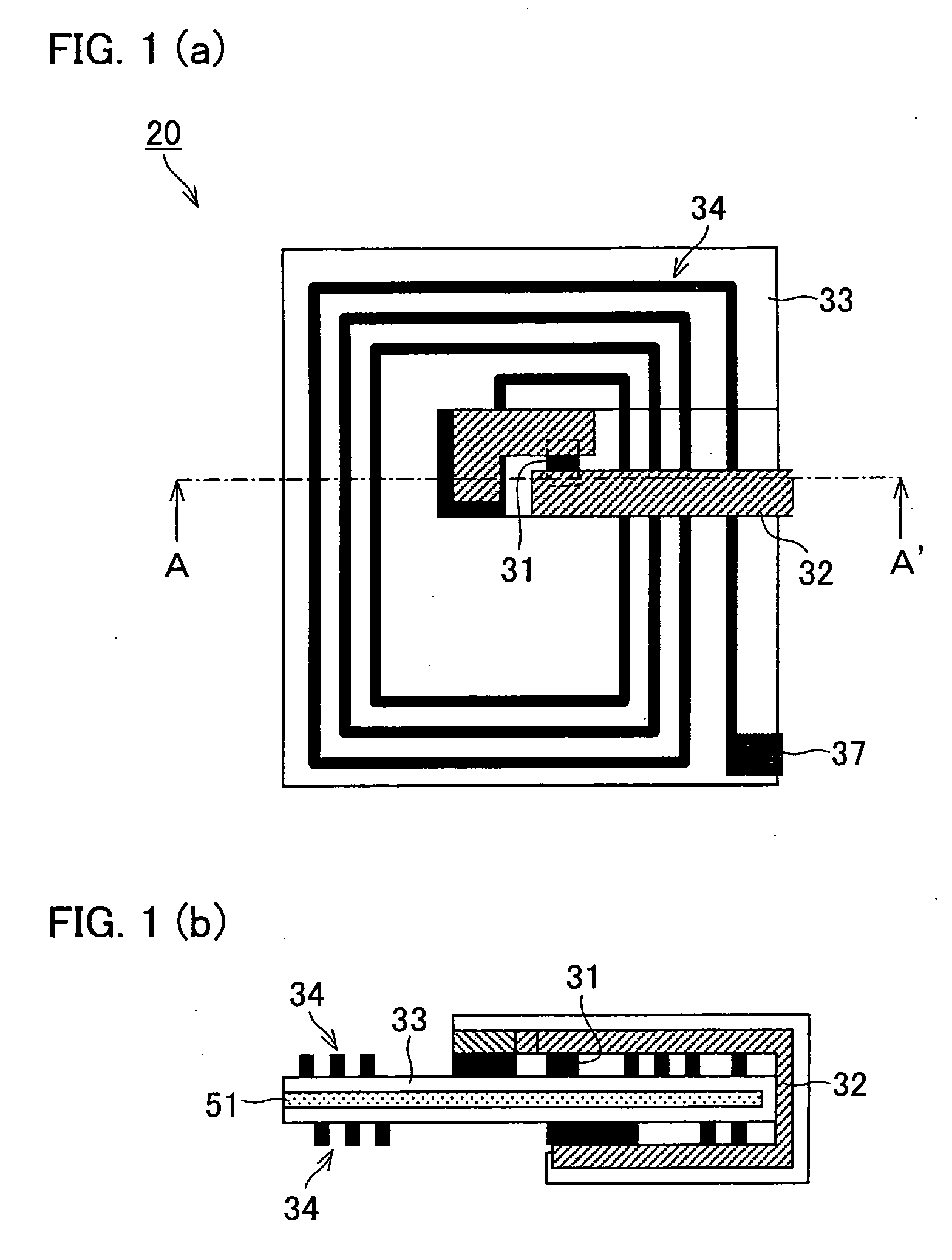
[0039] One embodiment of the present invention will be described below with reference to FIGS. 1(a) through 4(b) and FIG. 6.

[0040] FIGS. 1(a) and 1(b) show a thin IC tag according to one embodiment of the present invention. FIG. 1(a) is an overhead plan view of the thin IC tag according to the present embodiment, and FIG. 1(b) is a cross-sectional view illustrating the thin IC tag which is shown in FIG. 1(a) and which is taken along the line A-A′. As shown in FIG. 1(a), a thin IC tag 20 according to the present invention includes: a flexible sheet 33, winding conductor patterns 34 serving as an antenna coil, an electronic part module 32 on which an IC chip 31 is mounted, and a connecting part 37.

[0041] Further, as shown in FIG. 1(b), the thin IC tag 20 is formed as follows. That is, an electronic part holding film is prepared by connecting, to respective ends of the winding conductor patterns 34 provided on the flexible sheet 33, the electronic part module 32 having the IC chip 31...

embodiment 2

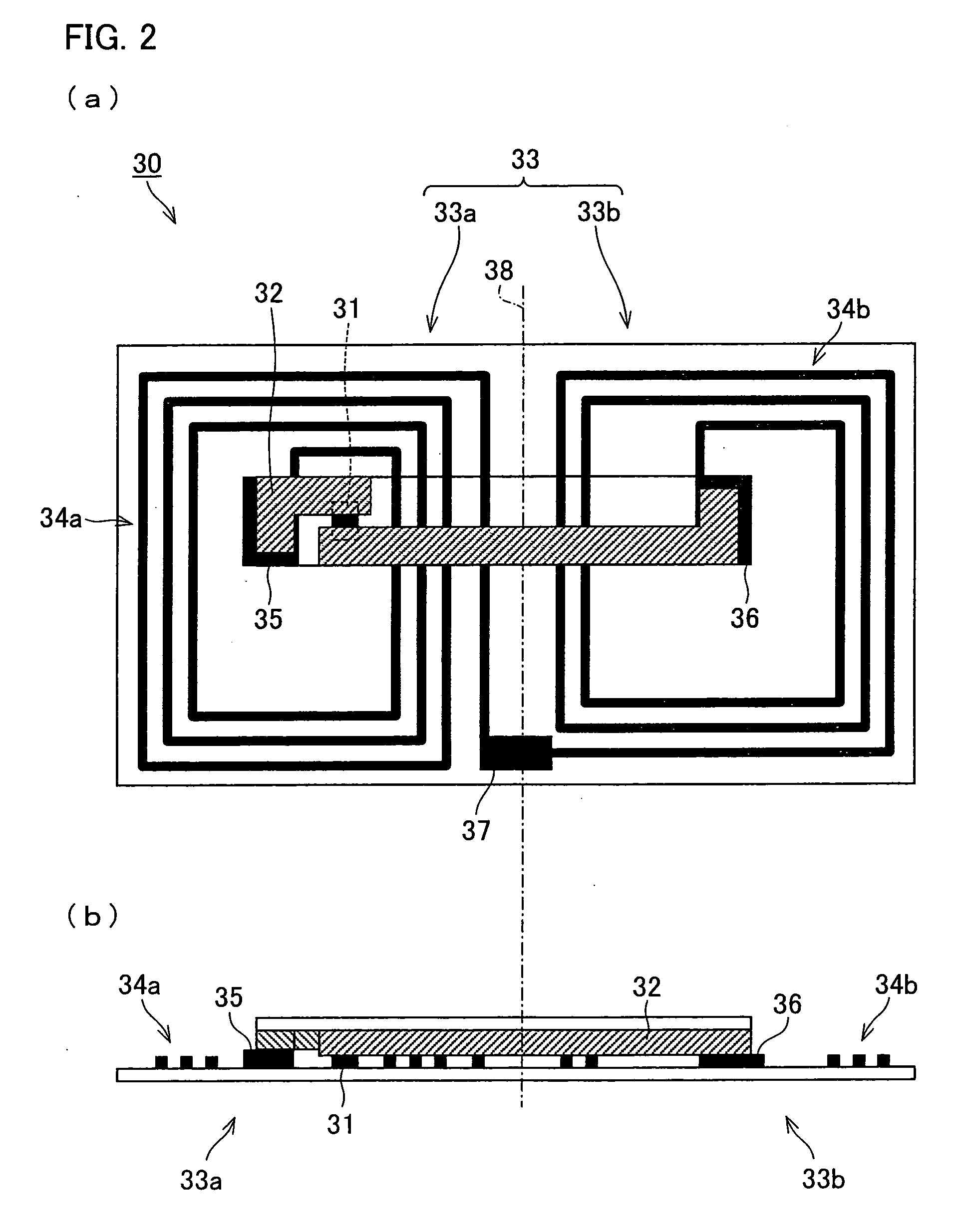
[0066] A thin IC tag according to another embodiment of the present invention and a method for manufacturing the thin IC tag will be described below with reference to FIGS. 5. For convenience of explanation, components having the same functions as those described in Embodiment 1 are given the same reference numerals, and description of the components is omitted. The present embodiment explains differences between Embodiment 1 and the present embodiment.

[0067] The thin IC tag described in Embodiment 1 is arranged as follows. That is, the adhesion layer 51 is formed on the surface of the electronic part holding film 30 opposite to the surface on which the electronic part module 32 is mounted, and the folding direction corresponds to the direction of the surface on which the adhesion layer 51 is formed. On the other hand, the thin IC tag according to the present embodiment is arranged as follows. That is, the adhesion layer 51 is formed on the surface of the electronic part holding fi...


PUM


Abstract

An electronic part holding film (30) includes an electronic part module (32) and winding conductor patterns (34a, 34b). The winding conductor patterns (34a, 34b) have ends in which terminal pads (35, 36) are formed and to which a connecting part (37) is not connected, respectively. The terminal pads (35, 36) are electrically connected to each other via the electronic part module (32). The electronic part holding film (30) is folded at a folding position (38). In this way, a thin IC tag (20) is manufactured. According to the thin IC tag (20), it is possible to provide a thin IC tag which does not increase the number of manufacturing steps and the manufacturing cost and on which an electronic part and the like can be mounted with ease.

Description

TECHNICAL FIELD [0001] The present invention relates to a flexible thin IC tag suitable for use, for example, in an IC label which can be provided in a slip and which can be read in a noncontact manner by using an induction field. Particularly, the present invention relates to (i) a thin IC tag for producing a small-size IC label and (ii) a method for manufacturing the thin IC tag. (Hereinafter, the IC label which can be provided in the slip is referred to as “slip-embedded type IC label”.) BACKGROUND ART [0002] For the purpose of promoting automation of distribution, it is important that a slip or the like attached to an individual article or the like can be read by machine. Conventionally, for this purpose, a bar code label representing the slip has been attached to the slip. [0003] However, in cases where the bar code label is read by using a so-called bar code reader, the bar code label and the bar code reader need to be highly precisely correlated with each other in terms of a ...

Claims


Application Information

Patent Timeline
Patent Type & Authority Applications(United States)
IPC IPC(8): G08B13/14B42D15/10G06K19/07G06K19/077H01Q1/22H01Q7/00H01Q7/02
CPCG06K19/07718G06K19/07749G06K19/07779H01Q7/00G06K19/07784H01Q1/22G06K19/07783G06K19/07G06K19/077H01Q7/02
Inventor KAWAI, WAKAHIRO
Owner ORMON CORP
Why Eureka
Try Eureka