
Dual CPU on-chip-debug low-gate-count architecture with real-time-data tracing

a low-gate-count, dual-core technology, applied in the field of microcontrollers, can solve the problems of high cost of expansion chips, and inability to debug various microcomputer applications, so as to reduce the amount of intrusion, reduce the cost of debugging, and increase the cost of the target microcontroller.

Active Publication Date: 2007-07-19
ATMEL CORP
View PDF9 Cites 10 Cited by
  • Summary
  • Abstract
  • Description
  • Claims
  • Application Information

AI Technical Summary

Benefits of technology

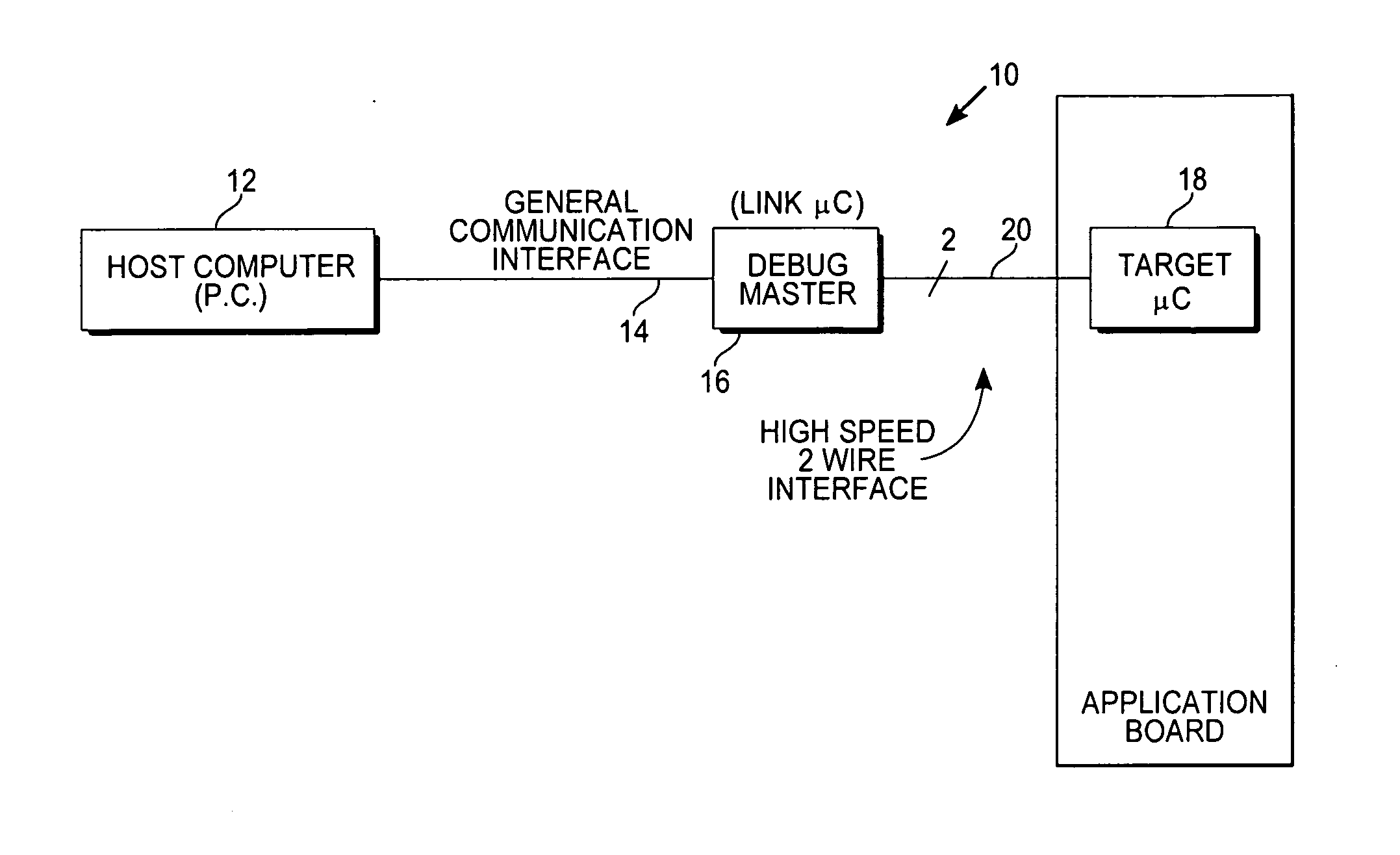
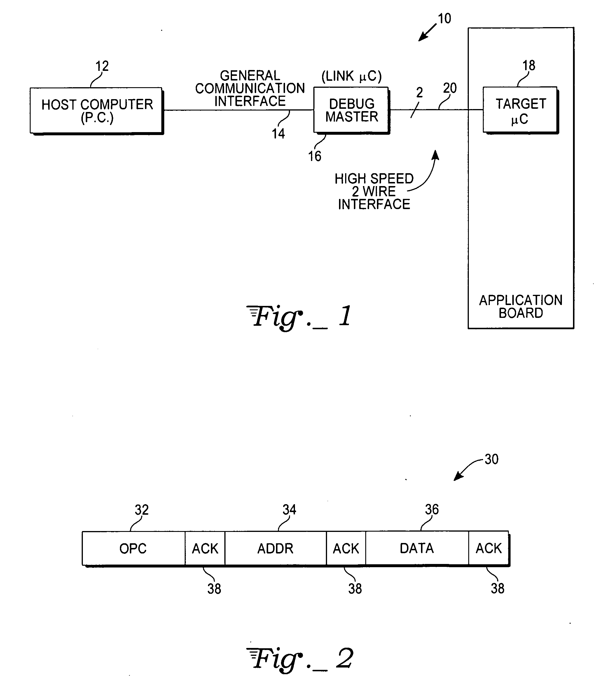
[0007] The present invention provides a Link microcontroller between a Host computer and a Target microcontroller. The Link microcontroller and the Target microcontroller are the same chip that is configured by a EEPROM fuse to be either a Link Master microcontroller or a Target Slave microcontroller. The Link microcontroller that functions as a master includes: 1) means for running an interface translator program between a Host computer and the Target microcontroller; 2) means for communicating with the Target microcontroller using a fast, 2-wire communication interface, and 3) means for communicating with the Host computer that is running monitor or debugging software for the application system in which the Target microcontroller is embedded. The Link microcontroller provides internal access to the Target microcontroller without using the I / O ports of the Target microcontroller. The Link microcontroller thereby provides an interface with the Host computer where the interface is that of a general purpose microcontroller with all of its available resources. This general purpose interface with the Host computer simplifies the task of a developer creating a monitoring / debug program that runs on the Host for debugging an application system that uses the Target microcontroller.
[0011] To reduce the amount of intrusion on the Target microcontroller required to implement a debug interface, that interface must be serial in nature. Several general purpose serial interfaces such as UART, SPI, and I2C already exist. The advantage of using a general purpose interface is that any existing device which implements that interface can act as the master of the debug interface. The disadvantage of using a general purpose interface is that these general purpose interfaces generally require large amounts of hardware on a Target device and require more software in a monitor to handle the communication, thereby increasing the cost of the Target microcontroller.
[0013] A custom hardware interface for the master is preferred over one that can be implemented in software on a generic master microcontroller. The advantages of using the Link-Target from the same chip design are that the achievable communication rate will be higher because the interface is implemented entirely in hardware and the development time for the debug system will be shorter because the system developer does not need to handle the low level details of the interface and can instead work at a higher level.

Problems solved by technology

Tying up several pins of a low-cost microcontroller along with the design time for providing suitable interfacing between the Host computer and the microcontroller are significant obstacles to successfully debugging various microcomputer applications.
For a low-cost, high volume microcontroller, such as a 8051 type, the expanded chip is expensive and impractical because of the low cost nature of the standard 8051 chip, while the expanded, special version would be a low volume, expensive chip.
The disadvantage of using a general purpose interface is that these general purpose interfaces generally require large amounts of hardware on a Target device and require more software in a monitor to handle the communication, thereby increasing the cost of the Target microcontroller.
Such a custom interface has no previously existing implementations, so there is no device to act as a master.
Using the same design is possible when at least 90% of the interface hardware is identical between the master and slave devices so that the cost increase for a dual use Link-Target chip is not great.

Method used


Image

  • Dual CPU on-chip-debug low-gate-count architecture with real-time-data tracing
  • Dual CPU on-chip-debug low-gate-count architecture with real-time-data tracing
  • Dual CPU on-chip-debug low-gate-count architecture with real-time-data tracing

Examples


Embodiment Construction

[0019]FIG. 1 shows a microcontroller debugging system 10 that includes a Host computer, such as a personal computer, 12 that is connected through a general communication interface 14 to a Link microcontroller 16. The Link microcontroller 16 functions as a debug master for a slave Target microcontroller 18. The Link microcontroller 16 and the Target microcontroller 18 communicate through a high-speed 2-wire interface 20. The Target microcontroller 18 is typically embedded in an application environment that includes an application circuit board that provides, for example, other integrated circuit packages, relays, sensors, actuators, etc., for a particular application. The Link microcontroller 16 and Target microcontroller 18 are different copies of the identical chip.

[0020] As previously mentioned, a microcontroller includes a microprocessor, code memory, peripherals, and port registers. The microprocessor itself includes an arithmetic / logic unit, SRAM / register files, an address con...


PUM


Abstract

The same microcontroller chip is configured to be either a Target version or a Link version of a microcontroller. The Target version runs an application program. To debug the Target microcontroller, the Link version of the microcontroller functions as a master debug microcontroller to the slave Target microcontroller running the application program. The Link microcontroller runs an interface translator program between a Host computer that runs a debug program, and the Target microcontroller. The Link microcontroller communicates with the Target microcontroller using a fast, 2-wire interface. The Link microcontroller communicates with the Host computer through a general purpose interface.

Description

TECHNICAL FIELD [0001] The invention relates to microcontroller and, in particular, to monitoring and debugging of a microcontroller application program. BACKGROUND ART [0002] A microcontroller, such as those in the various versions of the 8051 family of microcontrollers, includes a microprocessor, code memory, peripherals, and port registers mounted on a single chip. The microprocessor includes an arithmetic / logic unit, SRAM / register files, an address controller, a program counter, etc. [0003] To find various run-time errors in a microcontroller application that includes a microcontroller and other associated hardware, a debugger system is used. A debugger program runs on a Host computer and executes a host program for the purpose of finding run-time errors. Such errors are often not apparent until a debug program is either actually executed in a Target microcontroller system or is executed in a simulator for the Target microcontroller system. A debugger system provides various dia...

Claims


Application Information

Patent Timeline
Patent Type & Authority Applications(United States)
IPC IPC(8): G06F11/00
CPCG06F11/3648
Inventor LAMBRACHE, EMILFROEMMING, BENJAMIN F.AU, ANDREW K.
Owner ATMEL CORP
Learn More