

Programmable Resistive Ram and Manufacturing Method
- Summary
- Abstract
- Description
- Claims
- Application Information
AI Technical Summary
Benefits of technology
Problems solved by technology
Method used
Image

Examples
Embodiment Construction
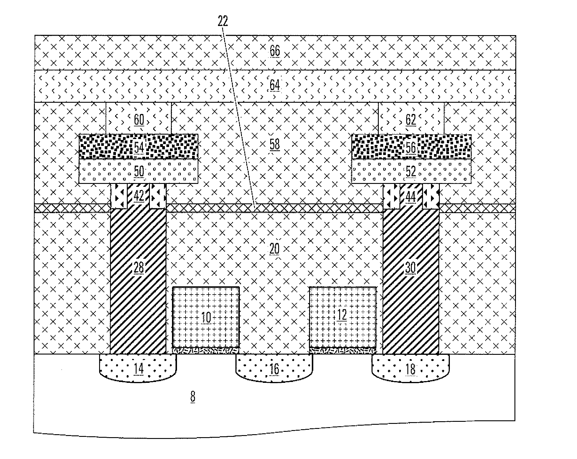
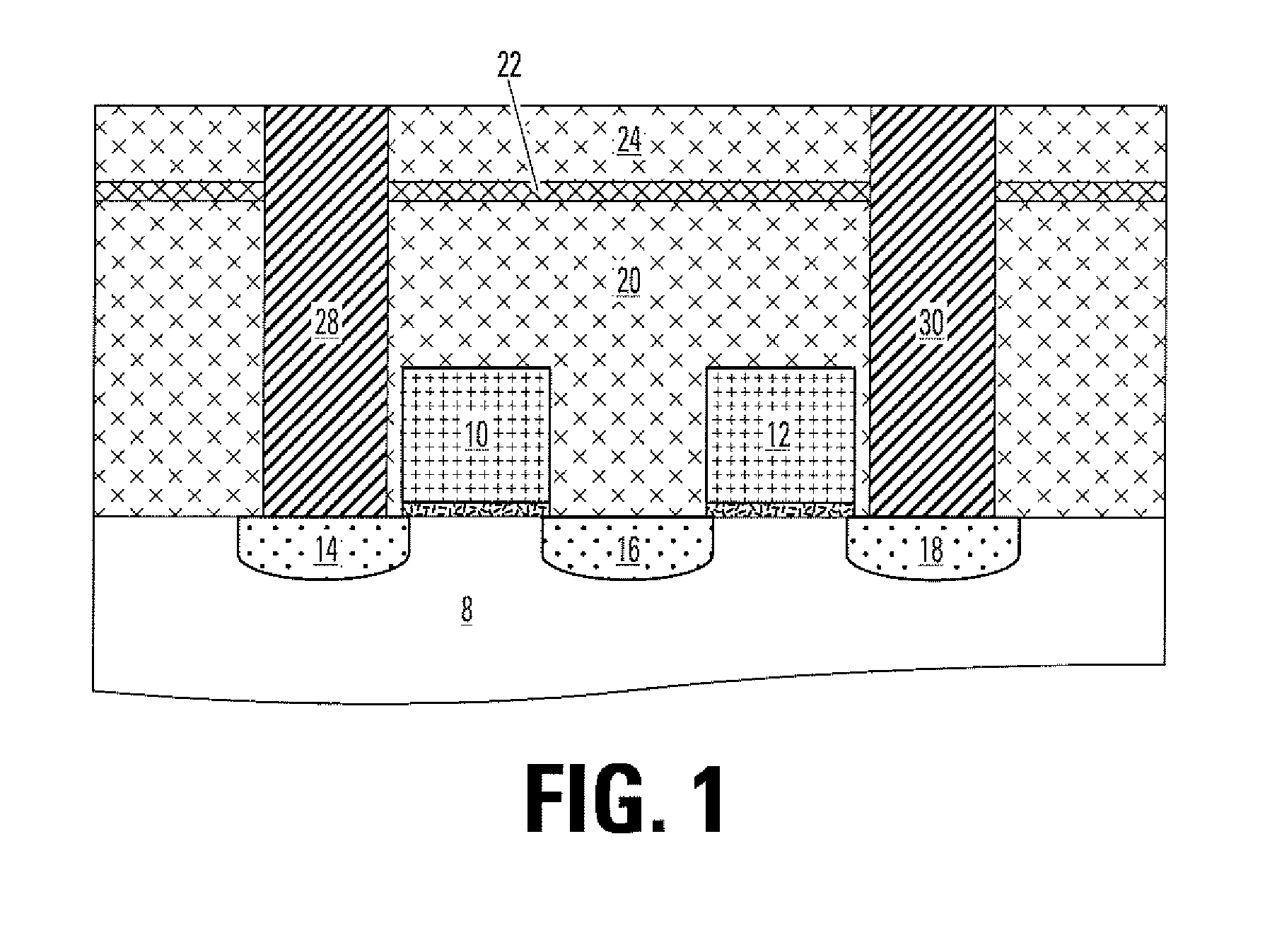
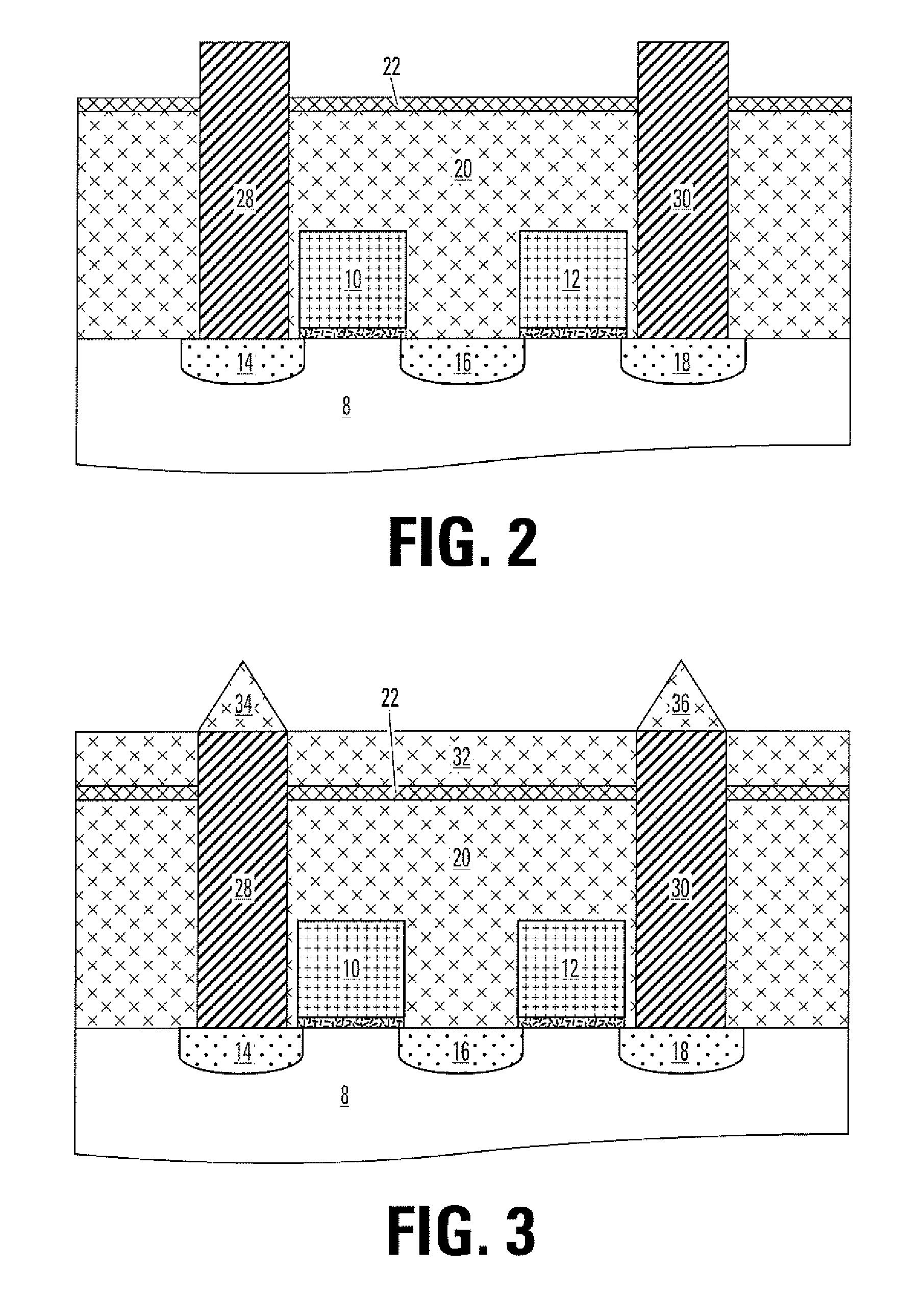
[0028] Various embodiments are directed at a manufacturing method for memory, such as nonvolatile embedded memory implementing programmable resistance RAM. Examples of resistance device RAM are resistance memory (RAM), polymer memory, and phase change memory (PCRAM). The cross-section is reduced of an upper portion of the interlayer contacts of programmable resistance RAM.
[0029]FIG. 1 is a cross-sectional view showing transistor structure to select particular programmable resistive RAM cells by row. The substrate 8 (which may also be an n-well or p-well) has source and drain regions 14, 16, and 18. The gates 10 and 12 are conductive rows which selectively access the programmable resistive RAM cells, and induce a channel under the respective regions of the substrate 8 under the gates 10 and 12, between regions 14 and 16 and regions 16 and 18. Dielectric layers 20, 22, and 24 cover the substrate 8 and the gates 10 and 12. Interlayer contacts 28 and 30 physically and electrically conn...
PUM
 Abstract
Description
Claims
Application Information