Thin-film circuit device, method for manufacturing thin-film circuit device, and electronic apparatus

a technology thin film, which is applied in the direction of sealing/covering of cooking vessels, semiconductor/solid-state device details, cooking vessels, etc., can solve the problems of thermal stress in the substrate, failure and defects of thin film circuit device including a substrate prepared from a resin film, etc., to achieve low cost, reduce manufacturing cost, and low heat resistance

Active Publication Date: 2007-07-26
SEIKO EPSON CORP
View PDF2 Cites 26 Cited by
  • Summary
  • Abstract
  • Description
  • Claims
  • Application Information

AI Technical Summary

Benefits of technology

[0025]The method is effective in manufacturing the thin-film circuit device at low cost.
[0026]In the method, the low-strength region is preferably formed by etching the thin-film circuit layer. This allows the contact holes and the low-strength region to be formed in one step, resulting in a reduction in manufacturing cost.
[0027]The method preferably further includes fabricating the thin-film circuit layer on a heat-resistant substrate, releasing the thin-film circuit layer from the heat-resistant substrate, and then transferring the thin-film circuit layer to a flexible substrate. This technique is called a release transfer process and is useful in providing a thin-film circuit layer, including high-performance thin-film transistors fabricated at high temperature, on a resin substrate having low heat resistance.

Problems solved by technology

A thin-film circuit device including a substrate prepared from a resin film can have defects due to a difference in physical property between the substrate and a thin-film circuit layer.
In the thin-film circuit device, since such materials having different physical properties are joined to each other, a change in temperature causes thermal stresses in the substrate and the thin-film circuit layer because of the difference in linear expansion coefficient.
This causes the failure of the thin-film circuit device.
Therefore, the stress caused by distortion such as bending can break the thin-film circuit layer.
Large stresses are developed in the end portions thereof because of stress concentration; hence, the end portions thereof serve as weak points that may cause the breakage of the thin-film circuit device.

Method used


Image

  • Thin-film circuit device, method for manufacturing thin-film circuit device, and electronic apparatus
  • Thin-film circuit device, method for manufacturing thin-film circuit device, and electronic apparatus
  • Thin-film circuit device, method for manufacturing thin-film circuit device, and electronic apparatus

Examples


first embodiment

[0047]A thin-film circuit device according to a first embodiment of the present invention will now be described with reference to FIGS. 1 and 2.

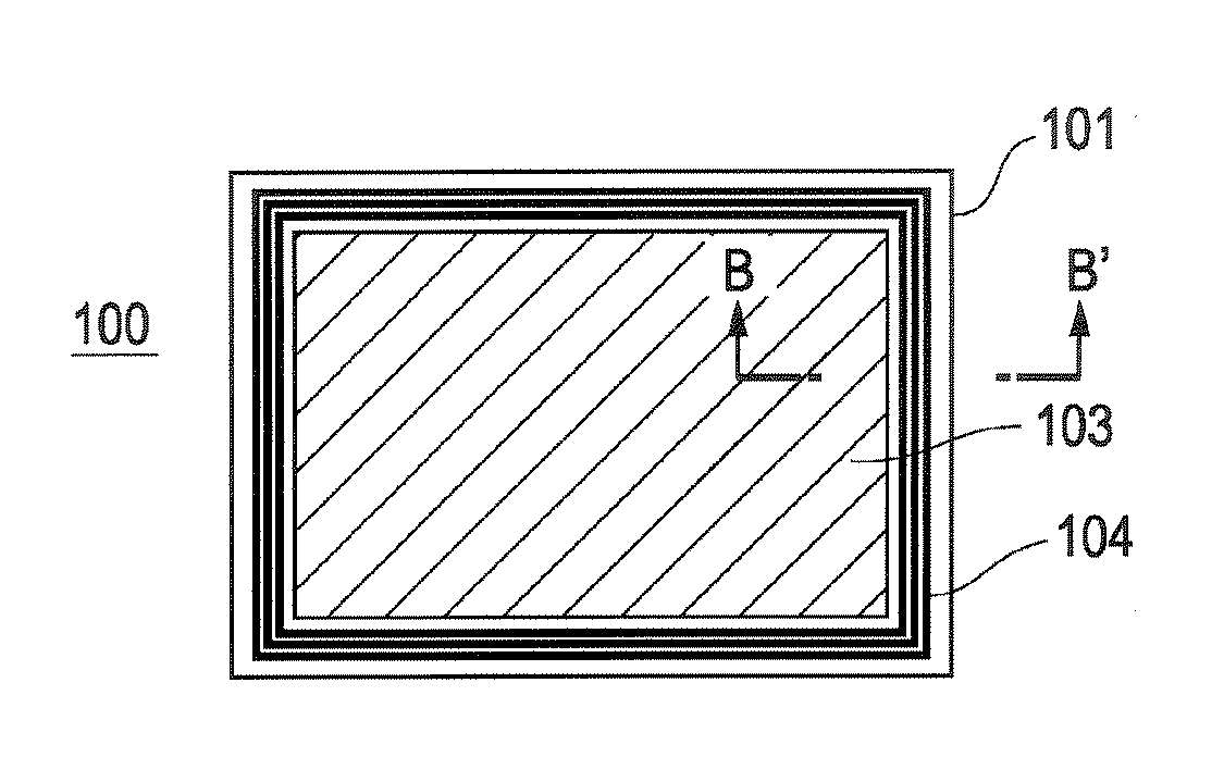
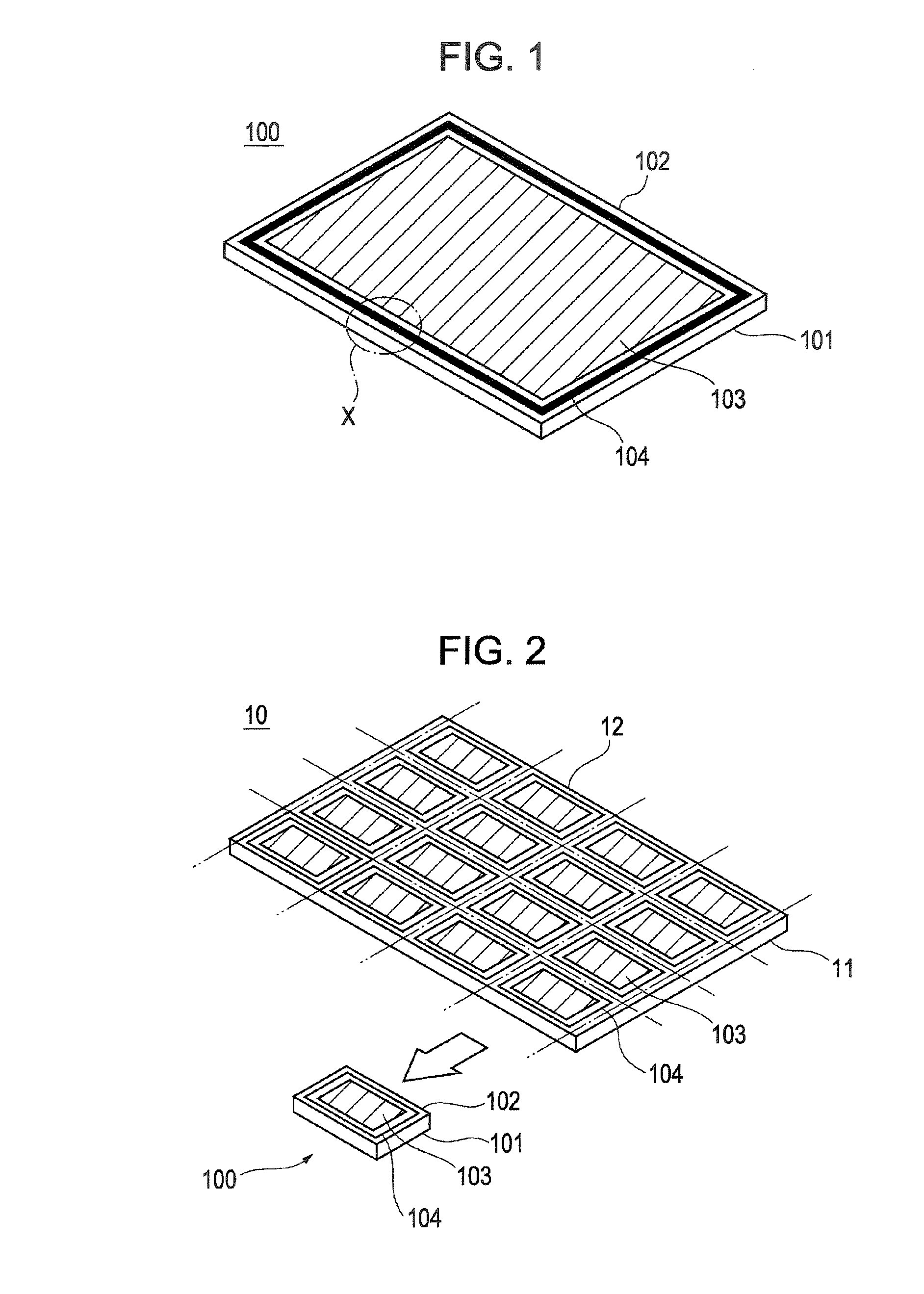
[0048]FIG. 1 is a perspective view of the thin-film circuit device. With reference to FIG. 1, the thin-film circuit device is represented by reference numeral 100 and includes a substrate 101 and a thin-film circuit layer 102 disposed thereon. In this embodiment, the thin-film circuit layer 102 has the same size as that of the substrate 101 and is formed on the substrate 101 so as to have an extremely small thickness. The thin-film circuit layer 102 may have a size different from that of the substrate 101.

[0049]The thin-film circuit layer 102 may be directly formed on the substrate 101 or may be formed on another substrate and then joined to the substrate 101 by the above release transfer process using an adhesive.

[0050]The thin-film circuit layer 102 includes an element region 103 and a low-strength region 104 surrounding the element region...

second embodiment

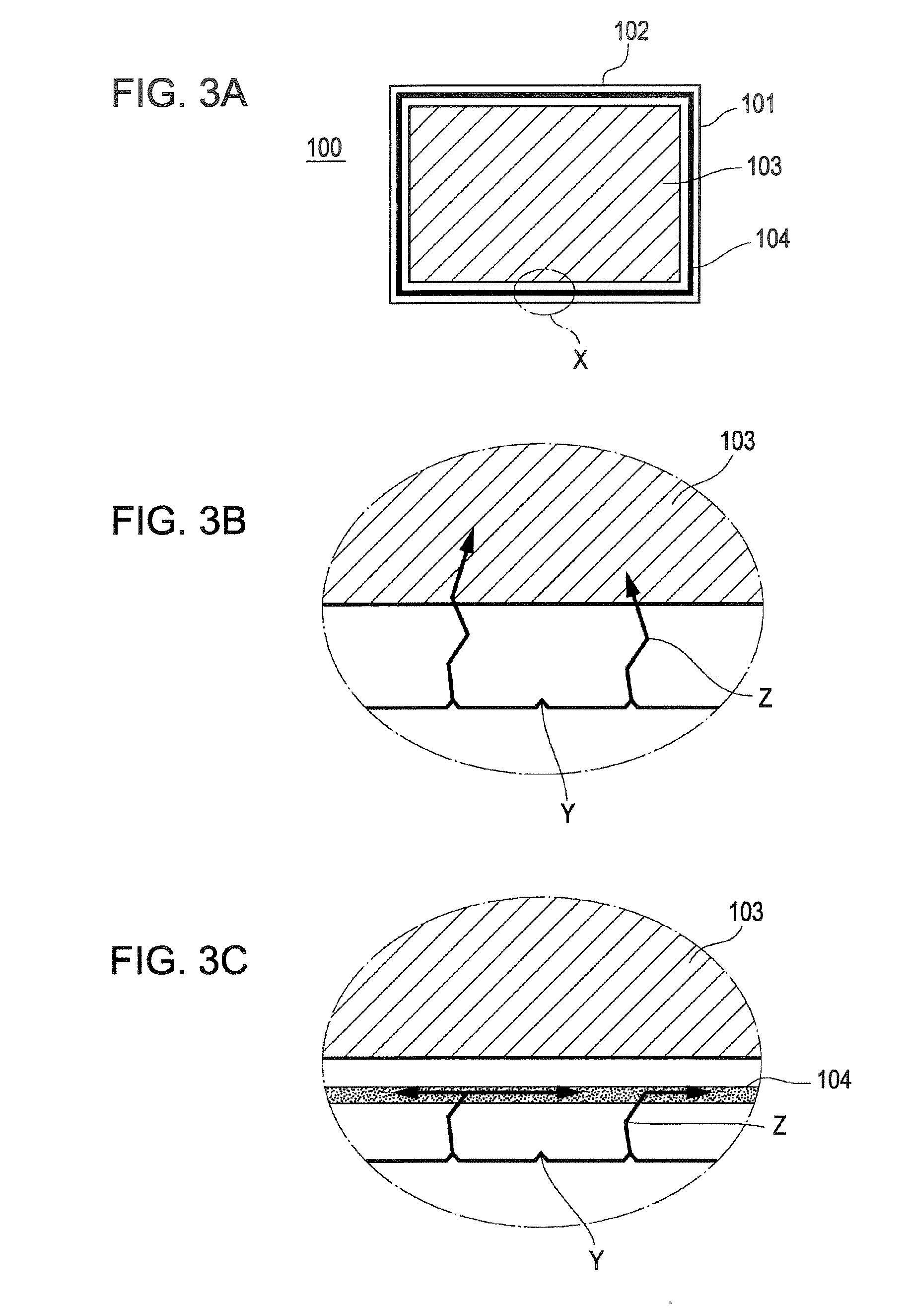
[0070]FIG. 5A shows a thin-film circuit device 100 according to a second embodiment of the present invention. The thin-film circuit device 100, as well as that of the first embodiment, includes a substrate 101 and a thin-film circuit layer 102 including an element region 103 and a low-strength region 104 surrounding the element region 103. The low-strength region 104 has a plurality of grooves.

[0071]FIGS. 5B to 5C are enlarged sectional views of the thin-film circuit device 100, shown in FIG. 5A, taken along the line B-B′.

[0072]The grooves may have a rectangular or inverted trapezoidal shape in cross section as shown in FIG. 5B, a V shape in cross section as shown in FIG. 5C, or a semi-elliptical shape in cross section as shown in FIG. 5D. Alternatively, the grooves may have a semi-circular shape in cross section or may partly have any one of these shapes in cross section.

[0073]According to this configuration, even if cracks are developed in an end portion of the thin-film circuit d...

third embodiment

[0084]A method for manufacturing a thin-film circuit device according to a third embodiment of the present invention will now be described with reference to FIGS. 7A to 7G. In the method, a silicon thin-film for forming planar thin-film transistors is used as an etching stopper in a step of forming grooves having a rectangular shape in cross section.

[0085]As shown in FIG. 7A, a protective layer 201 is formed on a substrate 101 by a CVD process or another process using silicon dioxide or another compound. A silicon layer is formed on the protective layer 201 by a CVD process or another process. The silicon layer is subjected to laser crystallization and then heat treatment, whereby the silicon layer is converted into a polysilicon layer 202.

[0086]As shown in FIG. 7B, the polysilicon layer 202 is patterned, whereby a transistor-forming region and a low-strength region 104 serving as an etching stopper region are formed. Silicon dioxide is deposited over these regions by a CVD process,...


PUM


Abstract

A thin-film circuit device includes a substrate and a thin-film circuit layer, disposed on the substrate, having an element region and a low-strength region. The element region includes thin-film elements. The low-strength region extends between an end portion of the thin-film circuit layer and the element region and has a mechanical strength less than that of the surroundings of the low-strength region.

Description

BACKGROUND[0001]1. Technical Field[0002]The present invention relates to a thin-film circuit device (thin-film semiconductor device) including a thin-film circuit layer, disposed on a flexible substrate, including semiconductor elements; a method for manufacturing such a thin-film circuit device; and an electronic apparatus including such a thin-film circuit device.[0003]2. Related Art[0004]Thin-film circuit devices include substrates; thin-film circuit layers, disposed on the substrates, including semiconductor elements; and other components. The substrates are usually prepared from single-crystal silicon wafers, quartz glass wafers, heat-resistant glass wafers, resin films, or the like. These wafers are selected depending on the required performance and functions of the thin-film circuit devices. In particular, the resin films are preferable because a substrate prepared from a resin film is thin and flexible and therefore a thin-film circuit device including the substrate is light...

Claims


Application Information

Patent Timeline
Patent Type & Authority Applications(United States)
IPC IPC(8): H01L21/76
CPCH01L27/1266H01L27/1248Y10S438/978H01L29/78603A47J27/026A47J27/04A47J36/06A47J37/0623A47J37/067
Inventor KODAIRA, TAIMEIUTSUNOMIYA, SUMIO
Owner SEIKO EPSON CORP
Why Eureka
Try Eureka