Wafer level package for surface acoustic wave device and fabrication method thereof

a technology of surface acoustic wave and wafer level, which is applied in the direction of basic electric elements, printing, writing units, etc., can solve the problems of increasing manufacturing costs and complicated manufacturing of saw filter b>10/b>, and achieve the effect of improving structur

Active Publication Date: 2007-08-02
SAMSUNG ELECTRONICS CO LTD
View PDF7 Cites 16 Cited by
  • Summary
  • Abstract
  • Description
  • Claims
  • Application Information

AI Technical Summary

Benefits of technology

[0009]The present invention has been conceived to solve the above-mentioned problems occurring in the prior art, and an aspect of the present i

Problems solved by technology

As a size of the SAW element 14 gets smaller, manufacturing of the SAW filter 10 becomes more complicated so that the manufacturing cost can increase.

Method used


Image

  • Wafer level package for surface acoustic wave device and fabrication method thereof
  • Wafer level package for surface acoustic wave device and fabrication method thereof
  • Wafer level package for surface acoustic wave device and fabrication method thereof

Examples


Embodiment Construction

[0041]Exemplary embodiments of the present invention will be described in detail with reference to the annexed drawings. In the drawings, the same elements are denoted by the same reference numerals throughout the drawings. In the following description, detailed descriptions of known functions and configurations incorporated herein have been omitted for conciseness and clarity. The described exemplary embodiments are intended to assist the understanding of the invention, and are not intended to limit the scope of the invention in any way.

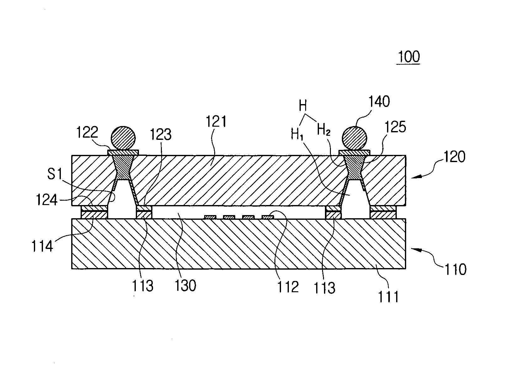
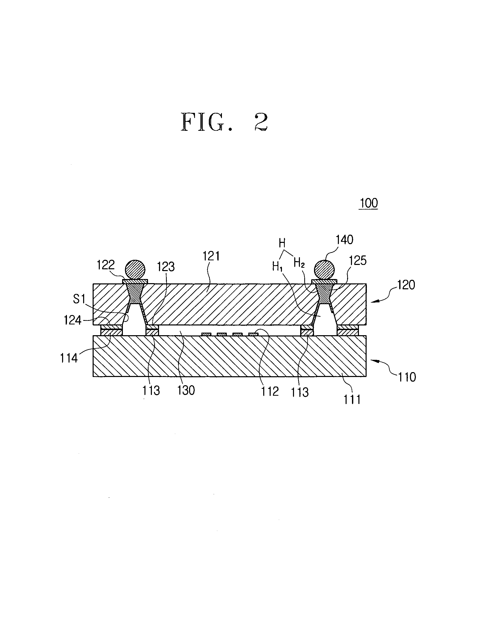
[0042]Referring to FIG. 2, a surface acoustic wafer (SAW) device wafer level package 100 comprises a SAW device 110 in which a SAW element 112 is formed on a top surface of a device wafer 111, and a packaging cap 120 bonded with a top surface of the SAW device 110. The packaging cap 120 is bonded with the SAW device 110 so that a cavity 130, which is formed between the packaging cap 120 and the SAW device 110, receives the SAW element 112.

[0043]The ...


PUM


Abstract

A wafer level package for a surface acoustic wave (SAW) device and a fabrication method thereof. The SAW device wafer level package includes a SAW device in which a SAW element is formed on a top surface of a device wafer, a cap wafer which is bonded with a top surface of the SAW device and has a viahole penetrating the cap wafer, and a conductive member to fill a part of the viahole. The viahole has a first via portion and a second via portion, the first via portion has a gradually smaller diameter from a bottom surface of the cap wafer until a certain depth, and the second via portion has a gradually greater diameter from the first via portion until a top surface of the cap wafer.

Description

CROSS-REFERENCE TO RELATED APPLICATIONS[0001]This application claims the benefit under 35 U.S.C. § 119 from Korean Patent Application No. 10-2006-9779 filed on Feb. 1, 2006, in the Korean Intellectual Property Office, the disclosure of which is incorporated herein by reference in its entirety.BACKGROUND OF THE INVENTION[0002]1. Field of the Invention[0003]The present invention relates to a surface acoustic wave device wafer level package that packages a surface acoustic wave device according to a wafer level packaging method, and a fabrication method thereof.[0004]2. Description of the Related Art[0005]As an electronic device is developed to be compact and high-efficient, its electronic parts need to also be compact and high-efficient. A surface acoustic wave (SAW) device is generally used as an electronic part such as a filter, a delay line, or an oscillator of an electronic device transmitting and receiving waves, and is also employed as a radio frequency (RF) part in a mobile pho...

Claims


Application Information

Patent Timeline
IPC IPC(8): H01L29/84
CPCH03H9/1092H01L2224/48091H01L2224/48227H01L2924/16195H01L2924/00014B43K23/012B43K23/12B43K24/02
Inventor LEE, MOON-CHULHWANG, JUN-SIKLIM, JI-HYUKKIM, WOON-BAE
Owner SAMSUNG ELECTRONICS CO LTD
Why Eureka
Try Eureka