Nano molecular modeling method

a molecular modeling and nano-scale technology, applied in nanoinformatics, instruments, computational theoretical chemistry, etc., can solve the problems of limiting the relevance of nano-tech systems to and the state-of-the-art electronic device modeling methods based on atomistic quantum mechanical first principles can only deal with systems involving roughly 1000 atoms or less

Inactive Publication Date: 2007-08-02
MCGILL UNIV
View PDF4 Cites 20 Cited by
  • Summary
  • Abstract
  • Description
  • Claims
  • Application Information

AI Technical Summary

Problems solved by technology

Such nano-tech modeling methods for electronic device properties do not yet exist today for lack of proper theoretical formalism and of associated modeling tool.
State-of-the-art electronic device modeling methods based on atomistic quantum mechanical first principles can currently only deal with systems involving roughly 1000 atoms or less, due to theoretical and numerical complexities.
This severely limits their relevance for most large scale nanotechnology systems.
Therefore, a challenge in the field of nanoelectronics is to develop adequate modeling methods.
Such modeling is heavily dependent on material and electronic parameters obtained by fitting to experimental data, which is becoming increasingly expensive and less reliable as device size continues to shrink.
Furthermore, due to fundamental limitations, traditional microelectronic devices theory and modeling methods are insufficient and even invalid when quantum effects are involved, for example in the case of charge transport at the up-coming scale between 30 nm and 50 nm.
However DFT methods of analysis of materials property has so far been applied to systems involving, in most cases, from a few tens to a few hundred atoms due to the complexity of the theory and its

Method used


Image

  • Nano molecular modeling method
  • Nano molecular modeling method
  • Nano molecular modeling method

Examples


Embodiment Construction

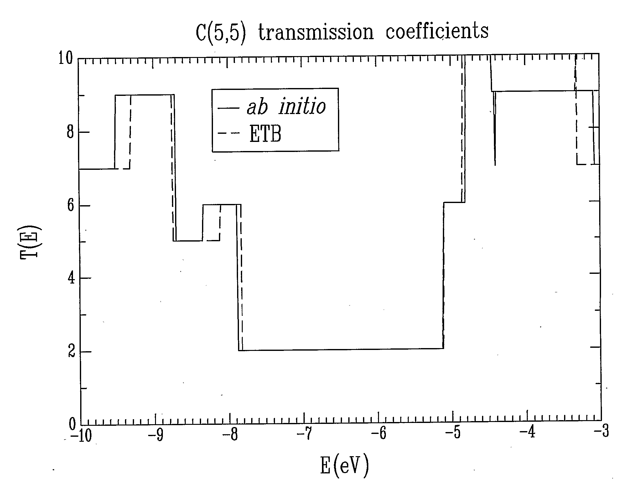
[0028] There is provided a multi-scale modeling method, which bridges a length scale gap between the two domains of current nano-systems discussed above, and therefore provides a powerful means to help developing a future generation of electronic devices, and has a wide range of applicability in the understanding and prediction of material, electronic and transport properties of nanoscale systems.

[0029] Based on previous methods developed so far as described hereinabove, the present method allows a qualitative leap, whereby nanosystems comprising from a single atom all the way to about 50 nm may be modeled.

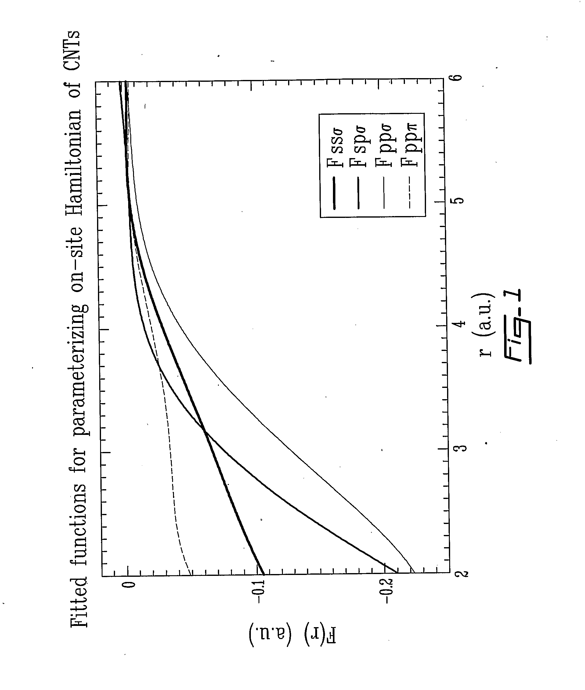
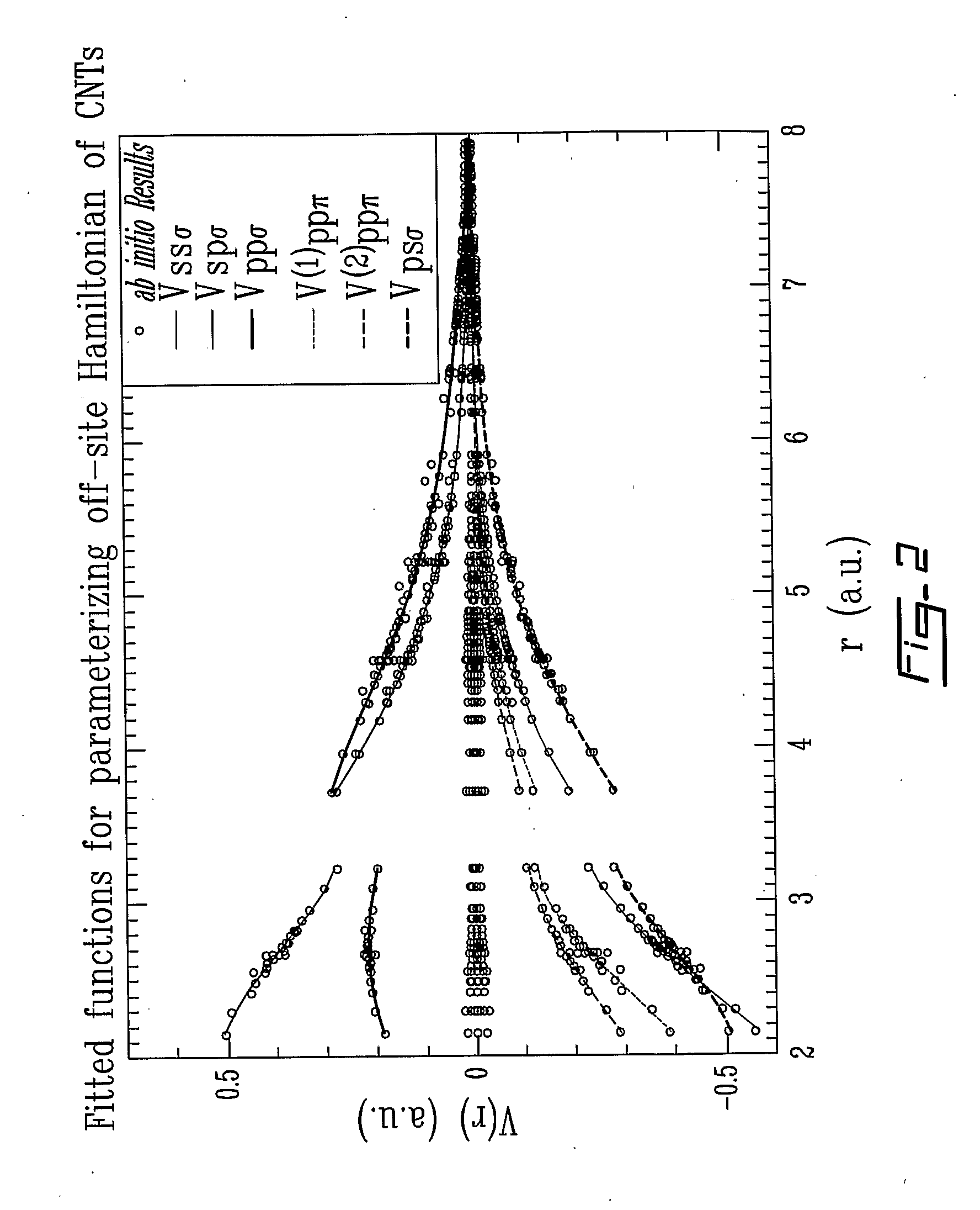
[0030] The present method for bridging length scales in nano-electronics modeling has been developed along four directions, as follows: for devices involving up to about a few thousands atoms, even up to 10,000 atoms, the method comprises using a self-consistent first principles atomistic formalism; for devices involving up-to one million atoms, the method comprises using a tigh...


PUM


Abstract

A nano-technology modeling method wherein a group of atoms and an interaction thereof to an open environment are defined by Hamiltonian matrices and overlap matrices, matrix elements of the matrices being obtained by a tight-binding (TB) fitting of system parameters to a first principles atomistic model based on density functional theory (DFT) with non-equilibrium density distribution.

Description

FIELD OF THE INVENTION [0001] The present invention relates to molecular modeling in the nano scale. More specifically, the present invention is concerned with a modeling method for nano systems. BACKGROUND OF THE INVENTION [0002] Electronic device modeling methods have allowed an incredible development rate of microtechnology, by allowing engineers to predict the performance of a technology emerging at the time. [0003] Similarly, nano-tech modeling methods would allow developing nano-electronics and nanotechnology to a full potential by enabling rapid design and validation of nano-scale materials and devices. Such nano-tech modeling methods for electronic device properties do not yet exist today for lack of proper theoretical formalism and of associated modeling tool. [0004] As people in the art are well aware of, the properties of electronic systems at a nano-meter scale are strongly influenced by quantum mechanical effects, and derive from conceptually different device structures...

Claims


Application Information

Patent Timeline
IPC IPC(8): G11C7/06G06F17/10
CPCG06F19/701B82Y10/00G16C10/00G16C60/00
Inventor GUO, HONG
Owner MCGILL UNIV
Why Eureka
Try Eureka