Mirror image shielding structure

Active Publication Date: 2007-08-09
IND TECH RES INST
View PDF9 Cites 4 Cited by
  • Summary
  • Abstract
  • Description
  • Claims
  • Application Information

AI Technical Summary

Benefits of technology

[0012]Accordingly, it is an object of the present invention to provide a mirror image shielding structure for reducing the parasitic effect between the electronic element and the ground shielding plane.
[0013]Another object of the present invention is to provide a mirror image shielding structure for reducing the vertical coupling effect between electronic elements.
[0014]Another object of the present invention is to prevent the vertical impact on the signal integrity of the embedded elements caused by the layout of the transmission lines

Problems solved by technology

Therefore, after the embedded elements are embedded therein through many different ways, a number of stray parasitic effects will occur.
Moreover, as an element gets closer and closer to elements (e.g., signal transmission lines, capacitors, and inductors) in the layers above and below, and as more composite materials are used, the overall coupling effect inevitably increases, which causes cross talk phenomena such as signal distortion, and further influences signal integrity (SI).
However, a large number of unnecessary parasitic effects 140 will thus occur due to the shielding plane, and parasitic capacitance is formed accordingly.
Moreover, using overall metal layers or overall metal meshes wastes materials and occupies a large area.
Therefore, though the capacitor can be effectively shielded, the high-frequency electrical characteristics thereof are destroyed due to the connection of the entire plane of metals, and a large area is occupied by the shielding structure.

Method used


Image

  • Mirror image shielding structure
  • Mirror image shielding structure
  • Mirror image shielding structure

Examples


Embodiment Construction

[0030]The content of the present invention is illustrated in detail below through specific embodiments with reference to accompanying drawings. Reference numerals mentioned in the specification refer to corresponding numbers in the drawings.

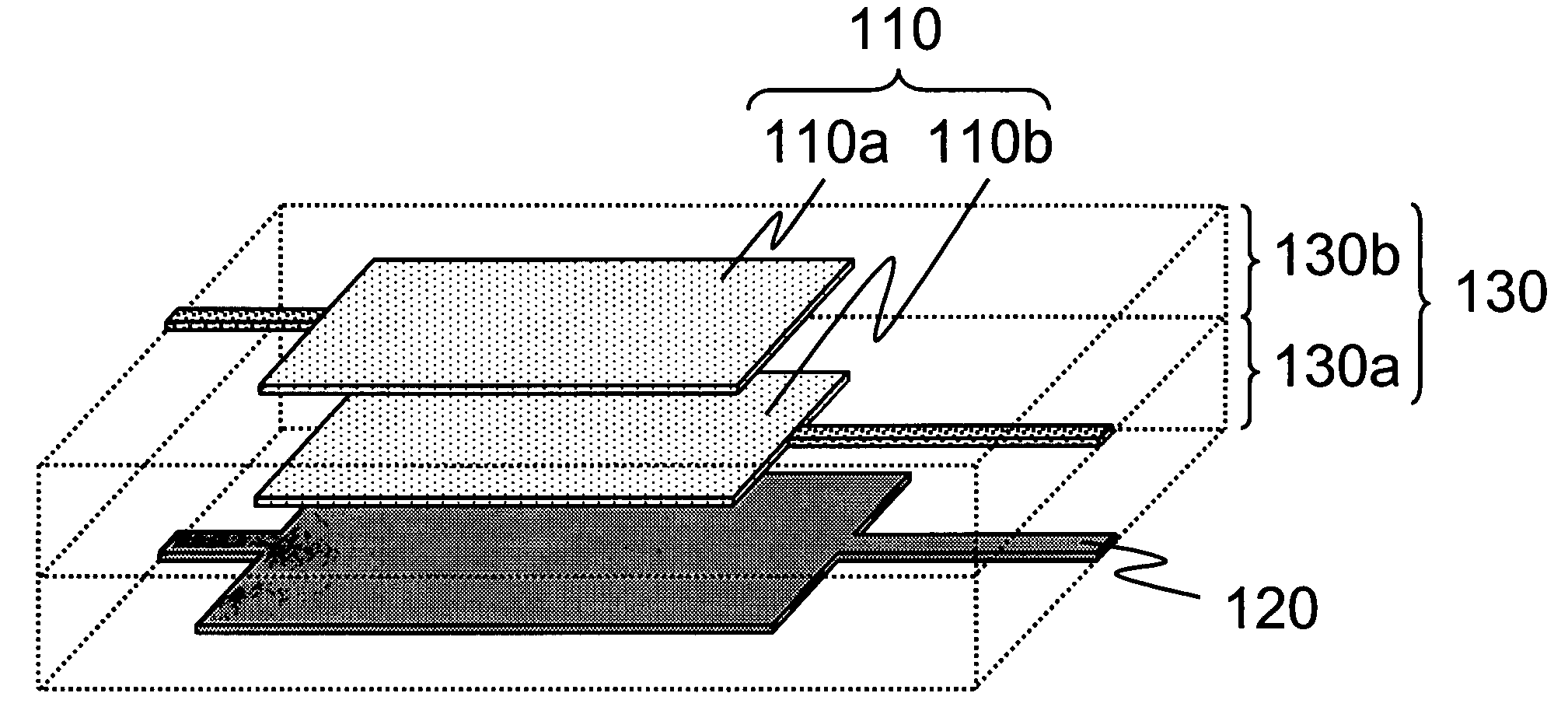
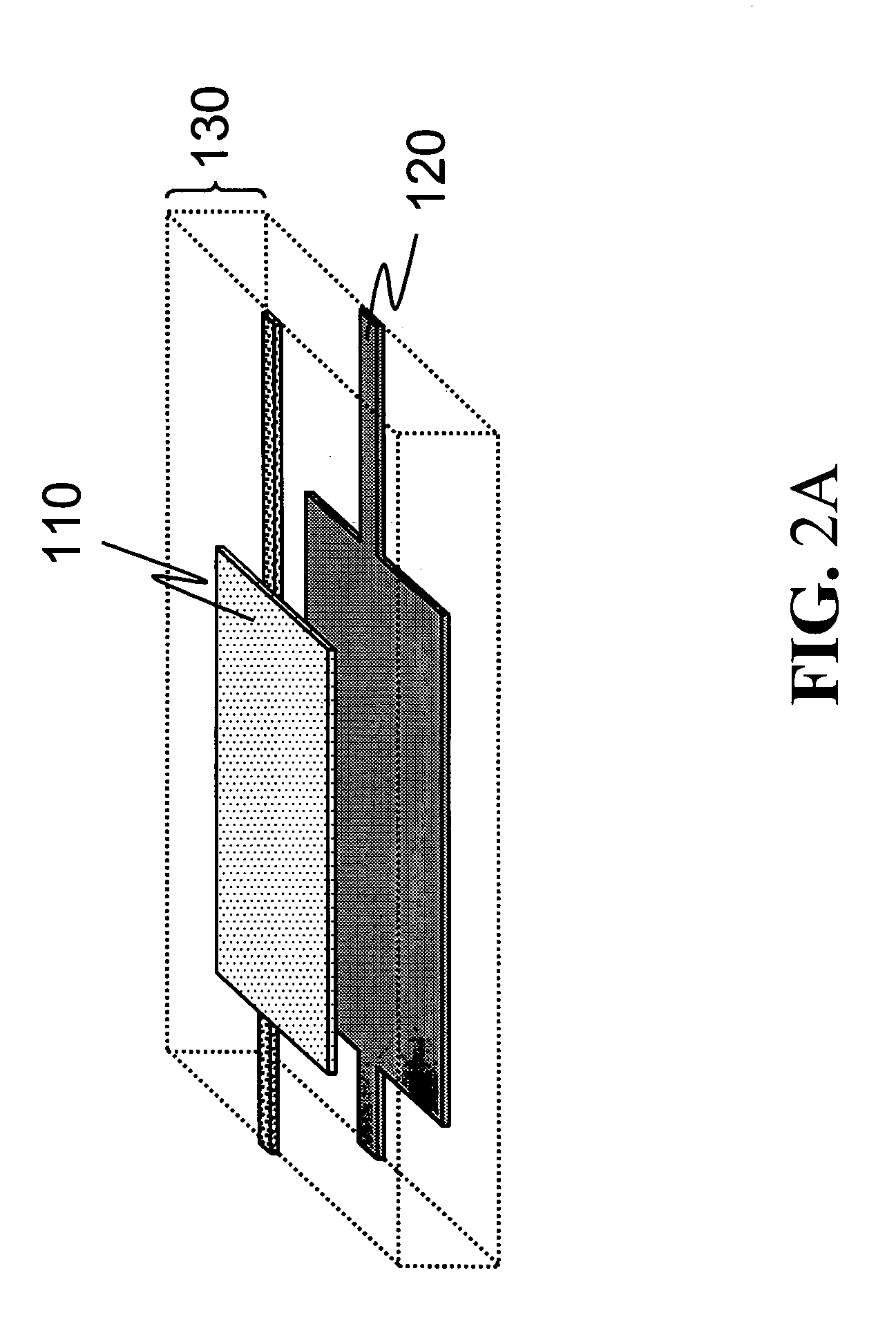
[0031]According to the present invention, two elements are isolated by a vertical metal shielding plane. In other words, the shape of the ground shielding plane can be similar to that of the vertical projection plane of the element, or that of the vertical projection plane of the element closest to the ground shielding plane.

[0032]FIGS. 2A, 2B, 2C, and 2D show the mirror image shielding structure of the present invention, which comprises a first electronic element 110 and a ground shielding plane 120. The ground shielding plane 120 is located under the first electronic element 110. The shape of the ground shielding plane 120 is similar to the projection shape of the first electronic element 110, and the horizontal size of the ground shielding pla...


PUM


Abstract

A mirror image shielding structure is provided, which includes an electronic element and a ground shielding plane below the electronic element. The shape of the ground shielding plane is identical to the projection shape of the electronic element, and the horizontal size of the ground shielding plane is greater than or equal to that of the electronic element. Thus, the parasitic effect between the electronic element and the ground shielding plane is effectively reduced, and the vertical coupling effect between electronic elements is also reduced. Furthermore, the vertical impact on the signal integrity of the embedded elements caused by the layout of the transmission lines is prevented.

Description

CROSS-REFERENCE TO RELATED APPLICATIONS[0001]This non-provisional application claims priority under 35 U.S.C. § 119(a) on Patent Application No(s). 095102900 filed in Taiwan, R.O.C. on Jan. 25, 2006, the entire contents of which are hereby incorporated by reference.BACKGROUND OF THE INVENTION[0002]1. Field of Invention[0003]The present invention relates to a shielding structure, and more particularly, to a mirror image shielding structure.[0004]2. Related Art[0005]Conventionally, passive components are disposed on the surface of the common printed circuit board (PCB) or on the surface of the substrate of semiconductor chips. However, with the development trend towards high functionality and small size of electronic products, the lamination technique for circuit boards has come to require the features of thin thickness, multiple layers, and high-density, and so on. Therefore, to create more space and to improve the multi-functionality of the module in a limited substrate area, the ci...

Claims


Application Information

Patent Timeline
IPC IPC(8): H04B3/28H05K9/00
CPCH05K1/0218H05K1/0224H05K1/0237H05K1/025H05K2201/09672H05K1/165H05K1/167H05K2201/0792H05K1/162
Inventor JOW, UEI-MINGSHYU, CHIN-SUNCHEN, CHANG-SHENGLEE, MIN-LINLAI, SHINN-JUH
Owner IND TECH RES INST
Why Eureka
Try Eureka