Light emitting element, light emitting device, and electronic device

Inactive Publication Date: 2007-08-16
SEMICON ENERGY LAB CO LTD
View PDF16 Cites 5 Cited by
  • Summary
  • Abstract
  • Description
  • Claims
  • Application Information

AI Technical Summary

Benefits of technology

[0023]Since a light emitting device of the present invention includes a light emitting element capable of low voltage drive, power consumption can be reduced. Further, since the light emitting device does not require a driver circuit with a high withstand voltage, it can be manufactured at low cost

Problems solved by technology

Therefore, inorganic EL elements have large power consumption, so it has been difficult to use

Method used


Image

  • Light emitting element, light emitting device, and electronic device
  • Light emitting element, light emitting device, and electronic device
  • Light emitting element, light emitting device, and electronic device

Examples


embodiment modes

[0030]Hereinafter, embodiment modes of the present invention will be described below in detail with reference to the accompanying drawings. However, the present invention is not limited to the description below, and those skilled in the art will appreciate that a variety of modifications can be made to the embodiment modes without departing from the spirit and scope of the invention. Accordingly, the present invention should not be construed as being limited to the embodiment modes described below.

embodiment mode 1

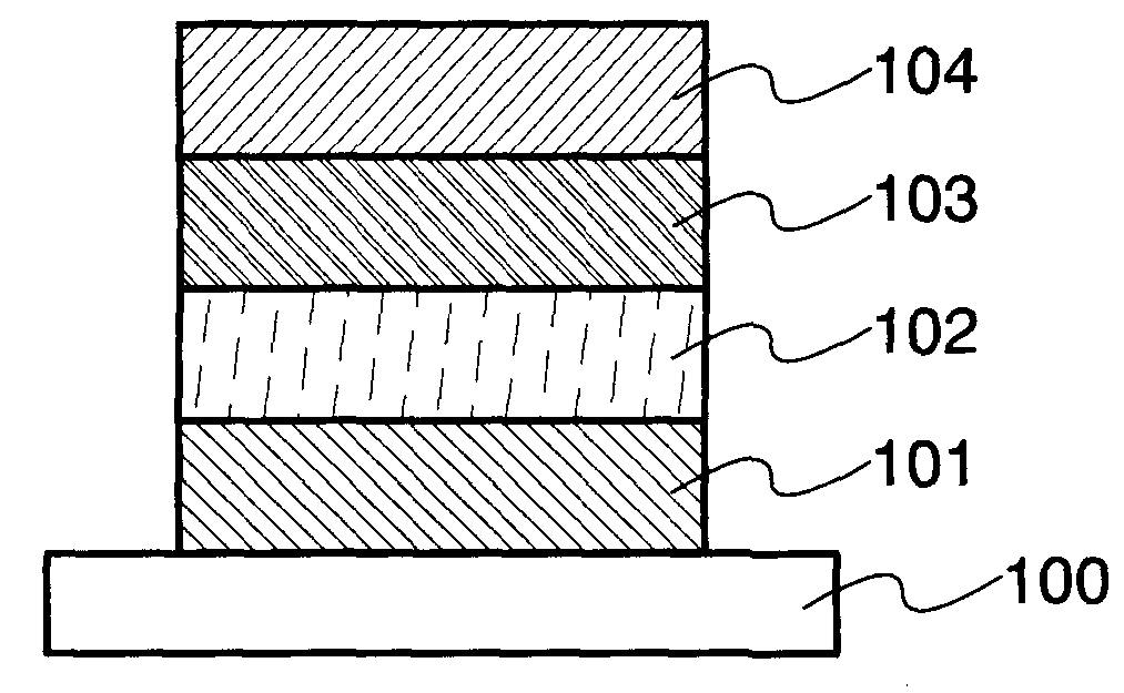
[0031]In this embodiment mode, a thin film light emitting element of the present invention will be described with reference to FIG. 1.

[0032]A light emitting element described in this embodiment mode has a structure which includes a first electrode 101 and a second electrode 104 which are formed over a first substrate 100. A p-type semiconductor layer 102 and an n-type semiconductor layer 103 are sandwiched between the first electrode 101 and the second electrode 104. Note that in the description of this embodiment mode, the first electrode 101 serves as an anode and the second electrode 104 serves as a cathode.

[0033]The substrate 100 is used as a support for the light emitting element. As the substrate 100, glass, quartz, plastic, or the like can be used, for example. Note that as long as the substrate serves as a support for the light emitting element in the manufacturing process, materials other than these can be used for the substrate.

[0034]As the first electrode 101 and the seco...

embodiment mode 2

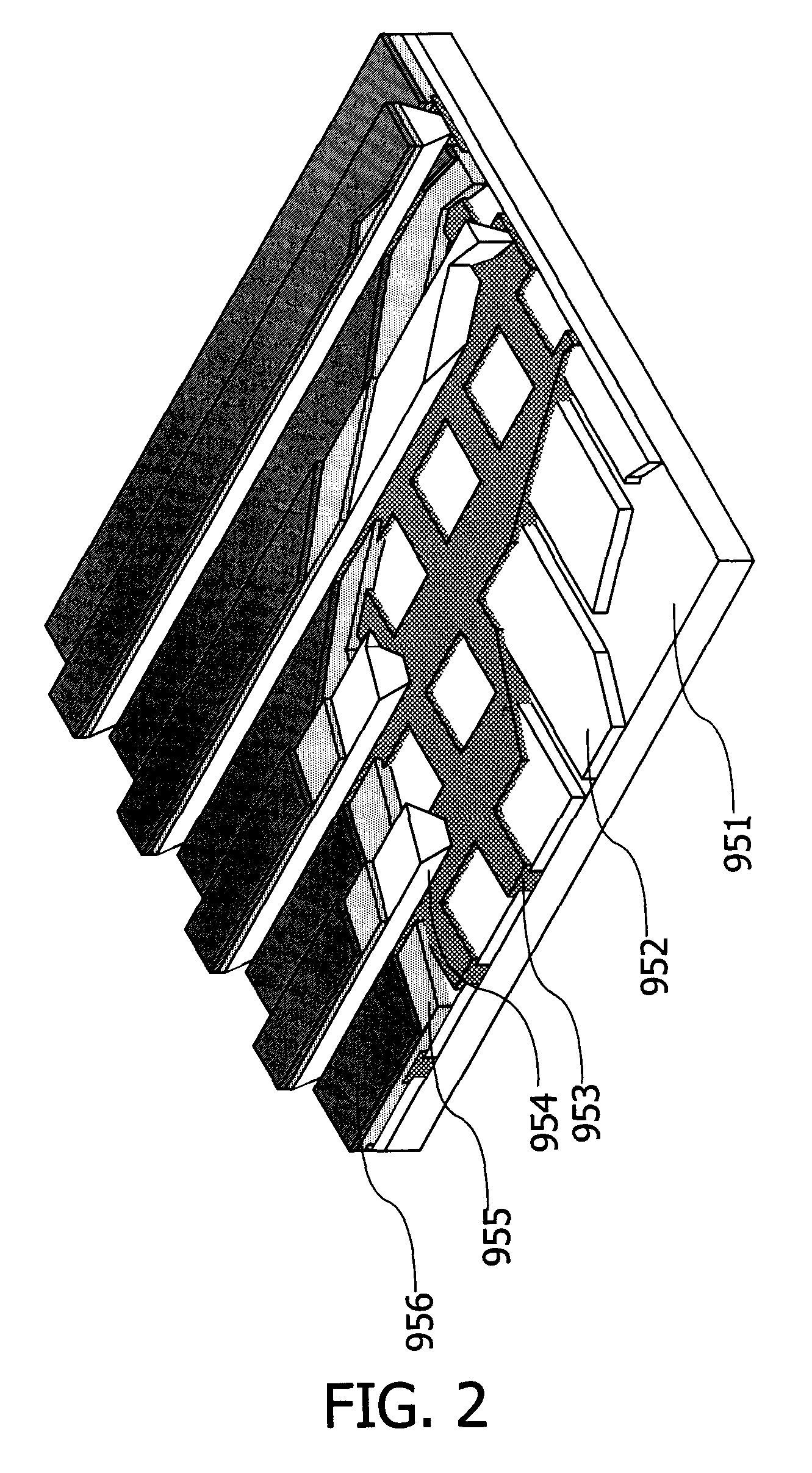
[0045]In this embodiment mode, a light emitting device having a light emitting element of the present invention will be described with reference to FIG. 2.

[0046]The light emitting device described in this embodiment mode is a passive light emitting device in which a light emitting element is driven without an element for driving, such as a transistor, being provided. FIG. 2 shows a perspective view of a passive light emitting device manufactured applying the present invention.

[0047]In FIG. 2, over a substrate 951, a semiconductor layer 955 is provided between an electrode 952 and an electrode 956. Note that the semiconductor layer 955 includes either the stacked layer structure of the p-type semiconductor layer and the n-type semiconductor layer described in Embodiment Mode 1, or a mixed layer of a p-type semiconductor and an n-type semiconductor.

[0048]An end portion of the electrode 952 is covered by an insulating layer 953. Further, over the insulating layer 953, a partition wall ...


PUM


Abstract

A light emitting element is provided, which comprises a pair of electrodes, a p-type semiconductor layer, and an n-type semiconductor layer. The p-type semiconductor layer and the n-type semiconductor layer are interposed between the pair of electrodes. The p-type semiconductor layer includes a first sulfide, and the n-type semiconductor layer includes a second sulfide. At least one of the p-type semiconductor layer and the n-type semiconductor layer includes a light emitting center.

Description

TECHNICAL FIELD[0001]The present invention relates to light emitting elements that employ electroluminescence. Further, the present invention relates to light emitting devices and electronic devices that have a light emitting element.BACKGROUND ART[0002]In recent years, concerning display devices in televisions, portable telephones, digital cameras and the like, there has been a demand for planar, slim display devices. As display devices which meet this demand, display devices which employ light emitting elements of a self-luminous type have been a focus of attention. An example of a light emitting element of a self-luminous type is a light emitting element utilizing electroluminescence. Such a light emitting element includes a light emitting material interposed between a pair of electrodes, and light emission can be obtained from the light emitting material by applying a voltage.[0003]Compared to a liquid crystal display, such a self-luminous light emitting element has advantages s...

Claims


Application Information

Patent Timeline
IPC IPC(8): H01L33/00H01L33/28
CPCC09K11/565C09K11/582H05B33/14C09K11/621H01L33/28C09K11/584
Inventor SAKATA, JUNICHIROYAMAMOTO, YOSHIAKIKAWAKAMI, TAKAHIROYOKOYAMA, KOHEIKATAYAMA, MIKIMATSUBARA, RIE
Owner SEMICON ENERGY LAB CO LTD
Why Eureka
Try Eureka