Pixel sensor structure including light pipe and method for fabrication thereof

a technology of pixel sensor and light pipe, which is applied in the direction of semiconductor devices, diodes, electrical devices, etc., can solve the problems of cmos image sensor color discrimination, pixel dimensions within cmos image sensors are certain to continue to decrease, and the performance of cmos image sensors continues to be compromised, so as to achieve enhanced reflection

Inactive Publication Date: 2007-08-16
GLOBALFOUNDRIES INC
View PDF16 Cites 98 Cited by
  • Summary
  • Abstract
  • Description
  • Claims
  • Application Information

AI Technical Summary

Benefits of technology

[0009] The invention provides a plurality of image sensor (e.g. CMOS image sensor) pixel structures and methods for fabrication thereof. The plurality of CMOS image sensor pixel structures and methods use a dielectric layer having an aperture therein registered with a photosensor region within a substrate over which is located the dielectric layer. The aperture yields a light pi...

Problems solved by technology

Such an off-axis capture, sensing and quantification of off-axis light generally compromises CMOS image sensor color discrimination.
Pixel dimensions within CMOS image...

Method used


Image

  • Pixel sensor structure including light pipe and method for fabrication thereof
  • Pixel sensor structure including light pipe and method for fabrication thereof
  • Pixel sensor structure including light pipe and method for fabrication thereof

Examples


first embodiment

[0031] The series of isolation regions 12 may comprise isolation regions including but not limited to local oxidation of silicon (LOCOS) isolation regions, shallow trench isolation regions (i.e., having a depth up to about 5000 angstroms) and deep trench isolation regions (i.e., having a depth up to about 60000 angstroms). Typically, the first embodiment uses shallow trench isolation regions that are located within shallow isolation trenches. The isolation regions 12 (whether located within shallow isolation trenches or deep isolation trenches) may comprise any of several dielectric materials. Typically included are oxides, nitrides and oxynitrides of silicon, as well as laminates thereof and composites thererof. Oxides, nitrides and oxynitrides of other elements are not excluded.

[0032] Typically, the series of isolation regions 12 is formed at least in part using a blanket layer deposition and planarizing method. Appropriate blanket layers may be formed using thermal or plasma oxid...

second embodiment

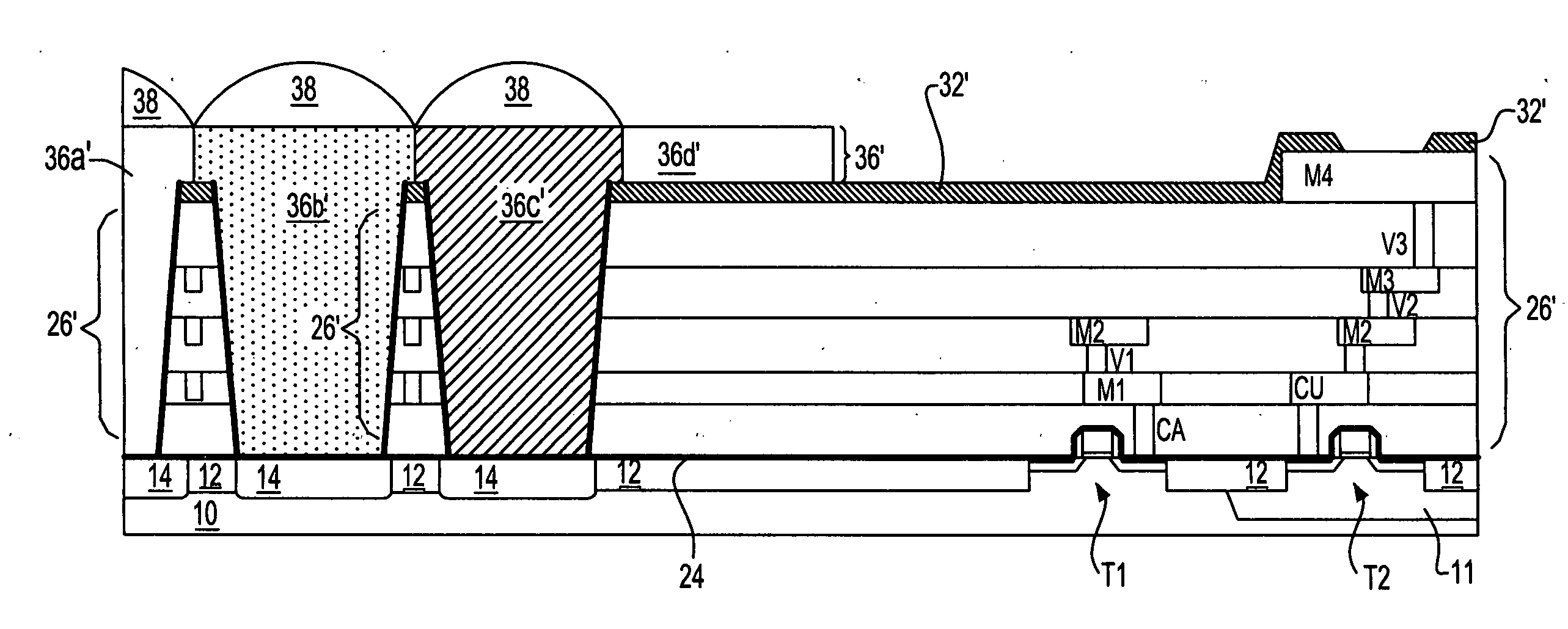
[0066] To minimize the foregoing scattering, an additional variation upon the second embodiment is provided within the context of the CMOS image sensor whose schematic cross-sectional diagram is illustrated in FIG. 8. The CMOS image sensor whose schematic cross-sectional diagram is illustrated in FIG. 8 correlates with the CMOS image sensor whose schematic cross-sectional diagram is illustrated in FIG. 7. However, as illustrated specifically within the insert to FIG. 8 an exception exists insofar as exposed edge and corner portions of the exposed ledge of interconnection layer M3′ are chamfered to provide a smoother surface that allows a reduction in light lost due to reflection or scattering from the top surface ledge of interconnection layer M3′. The resulting metallization layer is designated M3″. The capping layer is designated as CL′ and the combination is designated as M3′″.

[0067]FIG. 7 and FIG. 8 show a pair of schematic cross-sectional diagrams illustrating a pair of CMOS im...


PUM


Abstract

A pixel for an image sensor includes a photosensor located within a substrate. A patterned dielectric layer having an aperture registered with the photosensor is located over the substrate. A lens structure is located over the dielectric layer and also registered with the photosensor. A liner layer is located contiguously upon a top surface of the dielectric layer, and the sidewalls and bottom of the aperture. The liner layer provides for enhanced reflection for off-axis incoming light and enhanced capture thereof by the photosensor. When the aperture does not provide a dielectric layer border for a metallization layer embedded within the dielectric layer, an exposed edge of the metallization layer may be chamfered.

Description

CROSS-REFERENCE TO RELATED APPLICATIONS [0001] The present invention is related to commonly owned co-pending applications: (1) Ser. No. 10 / 904,807 (Docket BUR920040161US1), filed 30 Nov. 2004, titled “A Damascene Copper Wiring Image Sensor”; and (2) Ser. No. 11 / 275,171 (Docket BUR920050145US1), filed 16 Dec. 2005, titled “Funneled Light Pipe for Pixel Sensors.”BACKGROUND [0002] 1. Field of the Invention [0003] The invention relates generally to pixels within image sensors. More particularly, the invention relates to enhanced color discrimination pixels efficiently fabricated within CMOS image sensors. [0004] 2. Description of Related Art [0005] Complementary metal oxide semiconductor (CMOS) image sensors are gaining in popularity in comparison with other types of semiconductor image sensors, such as, in particular, charge coupled device (CCD) image sensors. In general, semiconductor image sensors are used as imaging components within various types of consumer and industrial products...

Claims


Application Information

Patent Timeline
IPC IPC(8): H01L27/14
CPCH01L27/14625H01L27/14632H01L27/14636H01L27/14689H01L27/14685H01L27/14687H01L27/14643
Inventor ACKERSON, KRISTIN M.ADKISSON, JAMES W.ELLIS-MONAGHAN, JOHN J.GAMBINO, JEFFREY P.HOAGUE, TIMOTHY J.JAFFE, MARK D.LEIDY, ROBERT K.MOON, MATTHEW D.PASSEL, RICHARD I.
Owner GLOBALFOUNDRIES INC
Why Eureka
Try Eureka