LED driver circuit

a driver circuit and driver technology, applied in the direction of instruments, static indicating devices, etc., can solve the problems of increasing the number of steps including resist formation, impurity ions implanted, and increasing the production cos

Inactive Publication Date: 2007-08-16
AL SID
View PDF7 Cites 13 Cited by
  • Summary
  • Abstract
  • Description
  • Claims
  • Application Information

AI Technical Summary

Benefits of technology

[0011] It is therefore an object of the present invention to provide an LED driver circuit that can suitably detect the minimum voltage and be made at low cost.
[0028] In the structure described above, the active devices that are employed in the minimum voltage selecting circuit comprise the p-MOSFET and the n-MOSFET. The MOSFET facilitate the formation of a depletion layer between the devices and the substrate, and ensures insulation between adjacent devices, so that it is unnecessary to take the effect of a parasitic transistor into consideration. Concretely, the above-mentioned p-MOSFET and n-MOSFET can be realized by a so-called single WELL structure in which a WELL is not formed in another WELL. Therefore, the parasitic transistor is not a problem, and the minimum voltage selecting circuit that is simple in structure can be formed at low cost.
[0031] In yet another preferred embodiment, the one pair of MOSFETs are the same channels and the switching signal is adapted to be inputted to a gate of one of the MOSFETs through an inverter. In this way, the input of the switching signal to the gate of the one of the MOSFETs is inverted, so that even if the MOSFETs are the same channels, they can realize the inverting operation.

Problems solved by technology

In a case where a diode is realized on a substrate, there is a structural problem that a parasitic transistor will be formed.
In a case where the double WELL structure is formed, there are problems that, in the production process for the double WELL structure, the number of the steps including forming of resists, implanting of impurity ions, etc. is increased and the production cost is therefore increased.
In this case, inaccurate voltages are inputted to the OPAMP, resulting in raising-voltage voltages being unsuitably controlled.

Method used


Image

  • LED driver circuit
  • LED driver circuit
  • LED driver circuit

Examples


Embodiment Construction

[0043] Preferred embodiments according to the present invention will be discussed hereinafter in the following order.

[0044] (1) Structure of an LED driver circuit;

[0045] (2) Structure of a minimum voltage selecting circuit;

[0046] (3) Variants; and

[0047] (4) Summary.

[0048] (1) Structure of an LED driver circuit:

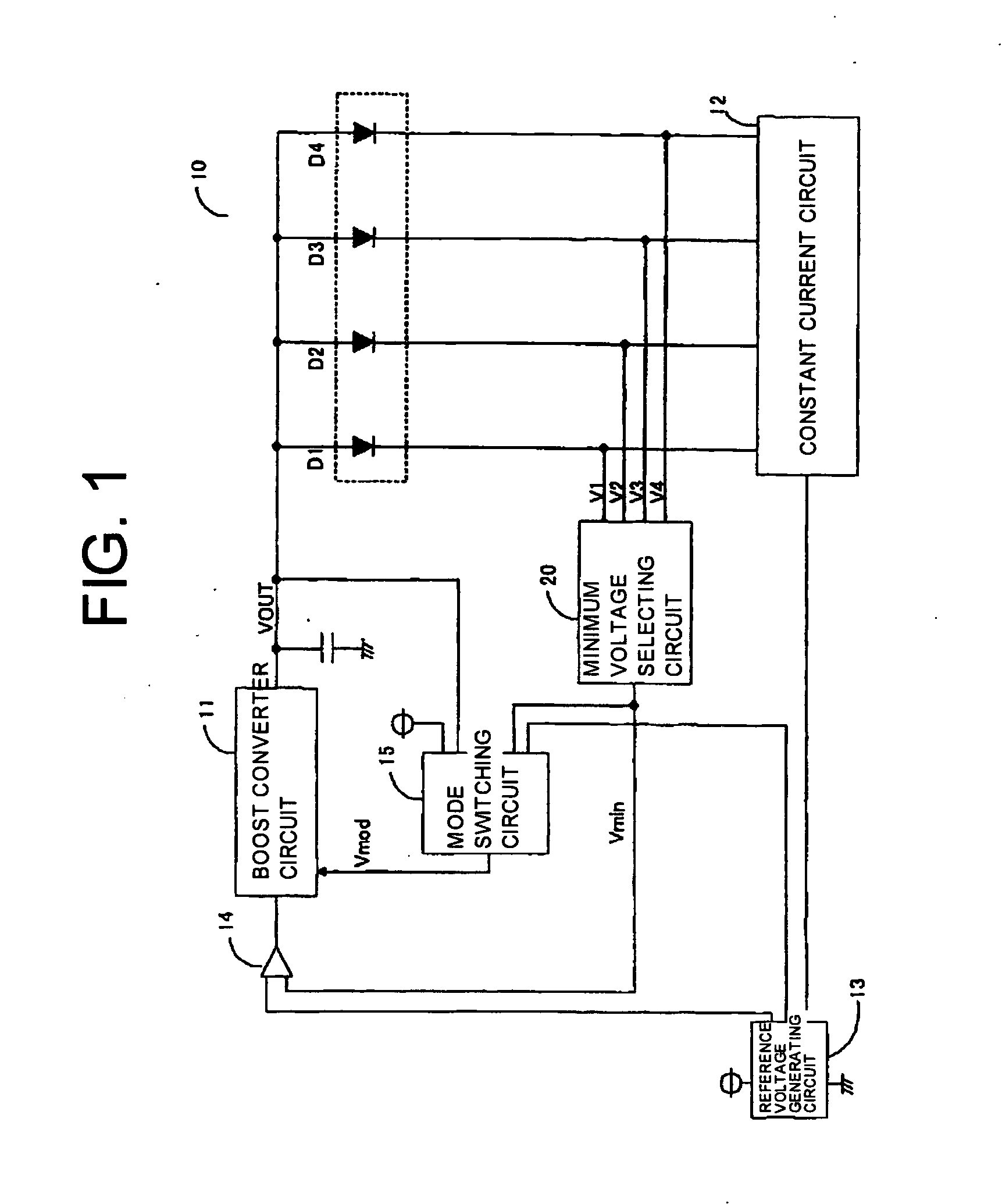
[0049]FIG. 1 is a schematic diagram illustrating an LED (Light Emitting Diode) driver circuit. In the LED driver circuit shown in the same Figure, a boost-converter circuit 11 is adapted to supply voltages to anodes of LEDs D1-D4 arranged in parallel. A constant current circuit 12 is a pump-type circuit and adapted to carry out control in such a manner to allow arbitrary current to flow through the respective LEDs D1-D4.

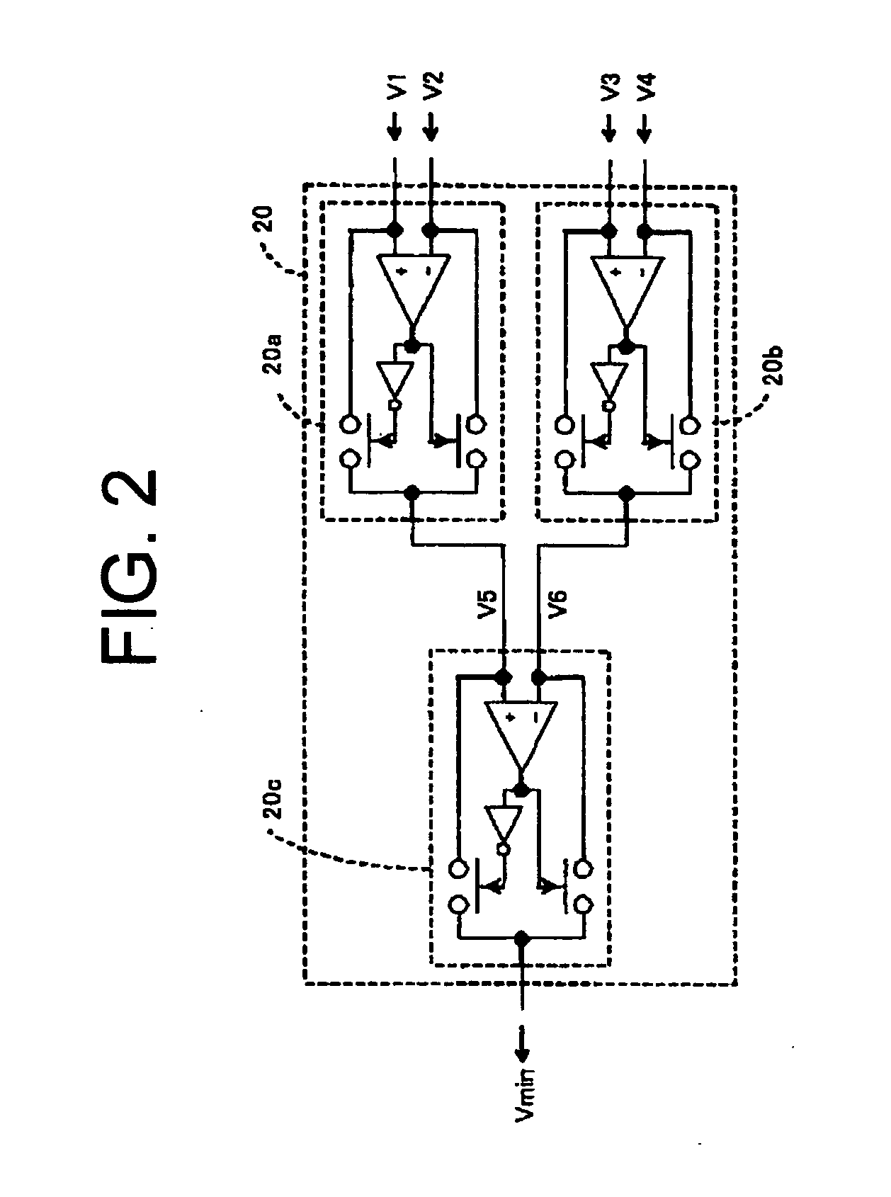
[0050] Cathode voltages V1-V4 of the LEDs Dl-D4 are adapted to be inputted to a minimum voltage selecting circuit 22 as estimation voltages V1-V4. The minimum voltage selecting circuit 22 is adapted to detect a minimum voltage Vmin from the estimation vo...


PUM


Abstract

Disclosed is an LED driver circuit that can suitably detect a minimum voltage and can be produced at low cost. A selector circuit is comprised of a comparator C, an inverter I and analogue switches. A minimum voltage selecting circuit can be constructed by causing the selector circuit and a circuit constructed in the same manner as the selector circuit is done, to be combined with each other. Therefore, the minimum voltage selecting circuit can be comprised of active devices that comprise only p-MOSFETs and n-MOSFETs. Moreover, as a semiconductor process structure, there may be employed a so-called single WELL structure in which a WELL is not formed in another WELL. The LED driver circuit is formed at low cost.

Description

BACKGROUND OF THE INVENTION [0001] 1. Field of the Invention [0002] The present invention relates to an LED driver circuit. [0003] 2. Description of the Related Art [0004] Hitherto, as LED driver circuit of this type, there is known an LED driver circuit that controls voltages to be applied to a plurality of LEDs, on the basis of a minimum voltage of cathode voltages of the LEDs (for example, U.S. Pat. No. 6,690,146). [0005]FIG. 3 of the patent document illustrates a circuit in which cathode electrodes of a plurality of diodes are respectively connected to cathode electrodes of the LEDs and anode electrodes are all energized and connected to an input of an OPAMP. Reference voltages generated by a reference diode are inputted to the other input terminal of the OPAMP. The OPAMP generates output voltages corresponding to voltage differences of these input voltages. A charge pump circuit controls voltages to be applied to the respective LEDs, according to the output voltages of the OPAM...

Claims


Application Information

Patent Timeline
IPC IPC(8): G09G3/32
CPCG09G3/3291
Inventor ITO, SATORUNISHIMURA, SEIJUN
Owner AL SID
Why Eureka
Try Eureka