Substrate processing apparatus

a processing apparatus and substrate technology, applied in the direction of photomechanical apparatus, instruments, printers, etc., can solve the problems of contaminated substrate edges, affecting the cleaning effect, so as to achieve easy control and high cleaning

Inactive Publication Date: 2007-08-16
SOKUDO CO LTD
View PDF10 Cites 48 Cited by
  • Summary
  • Abstract
  • Description
  • Claims
  • Application Information

AI Technical Summary

Benefits of technology

[0013] The first processing unit cleans the edge of the substrate before the exposure processing by the exposure device. In the first processing unit, the cleaning device cleans the edge of the substrate rotated by the rotation driving mechanism. At this time, the position correction device corrects the position where the substrate is cleaned by the cleaning device. Thus, the edge of the substrate can be uniformly cleaned. This prevents the edge of the substrate from being non-uniform in cleaning, thereby allowing a contaminant that has adhered to the edge of the substrate to be reliably removed.
[0064] Furthermore, when an organic film is formed on the substrate, components of the organic film on the substrate may be eluded or deposited during the exposure processing. By cleaning the edge of the substrate, therefore, the components eluded or deposited from the organic film on the substrate are previously eluded or deposited in the first processing unit during the exposure processing, so that an eluate or a deposit is cleaned away. Consequently, the components of the organic film on the substrate are prevented from being eluded or deposited during the exposure processing. This prevents the exposure device from being contaminated, thereby preventing a defective dimension and a defective shape of an exposure pattern.

Problems solved by technology

With recent increases in density and integration of devices, making finer resist patterns has become an important problem.
Therefore, making finer resist patterns has had a limitation.
Although the substrate is subjected to various types of film formation processing before the exposure processing, an edge of the substrate may, in some cases, be contaminated in the process of the film formation processing.
When the substrate is subjected to the exposure processing with the edge of the substrate thus contaminated, a lens of the exposure device may be contaminated, resulting in a defective dimension and a defective shape of an exposure pattern.

Method used


Image

  • Substrate processing apparatus
  • Substrate processing apparatus
  • Substrate processing apparatus

Examples


Embodiment Construction

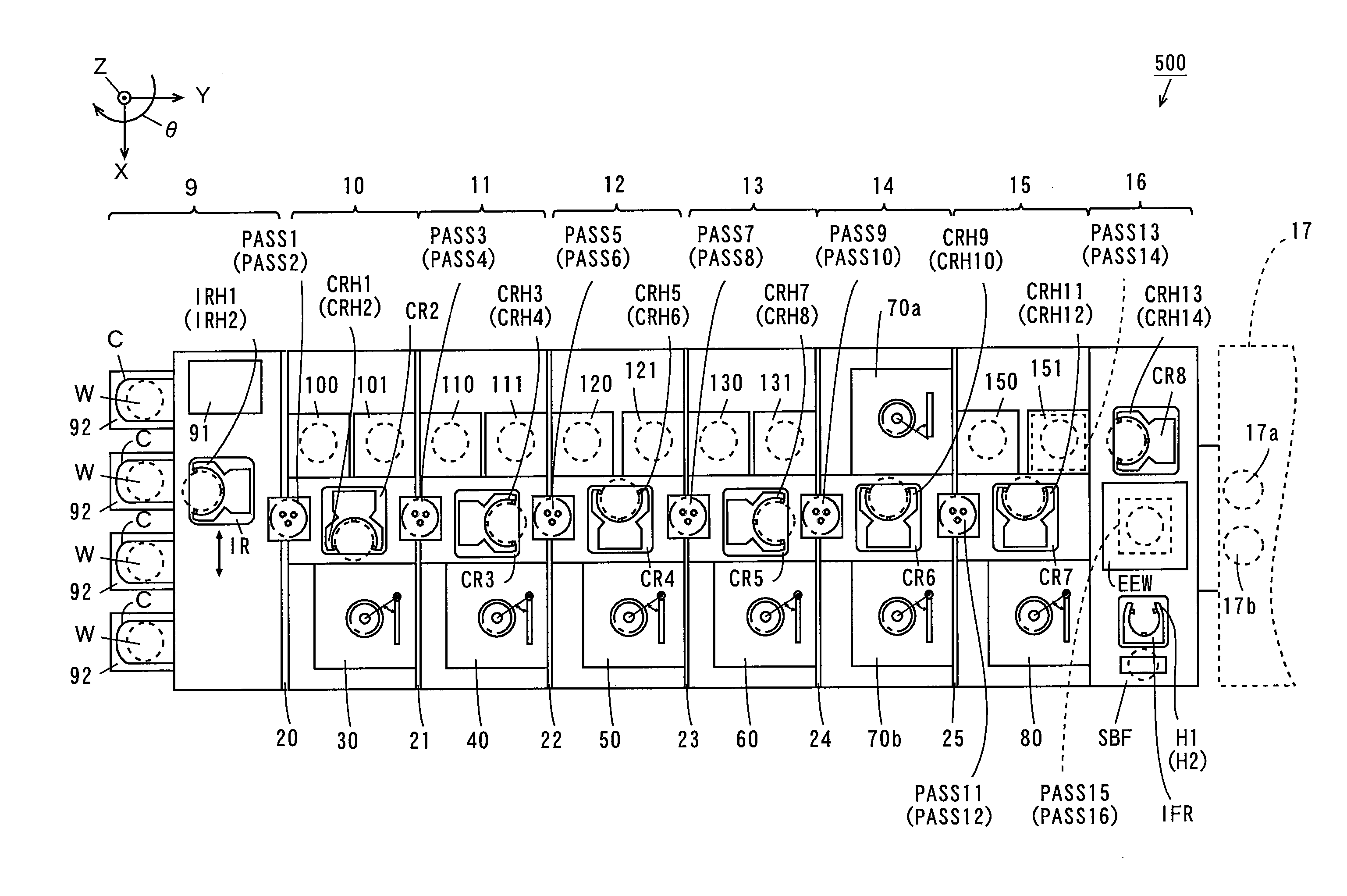
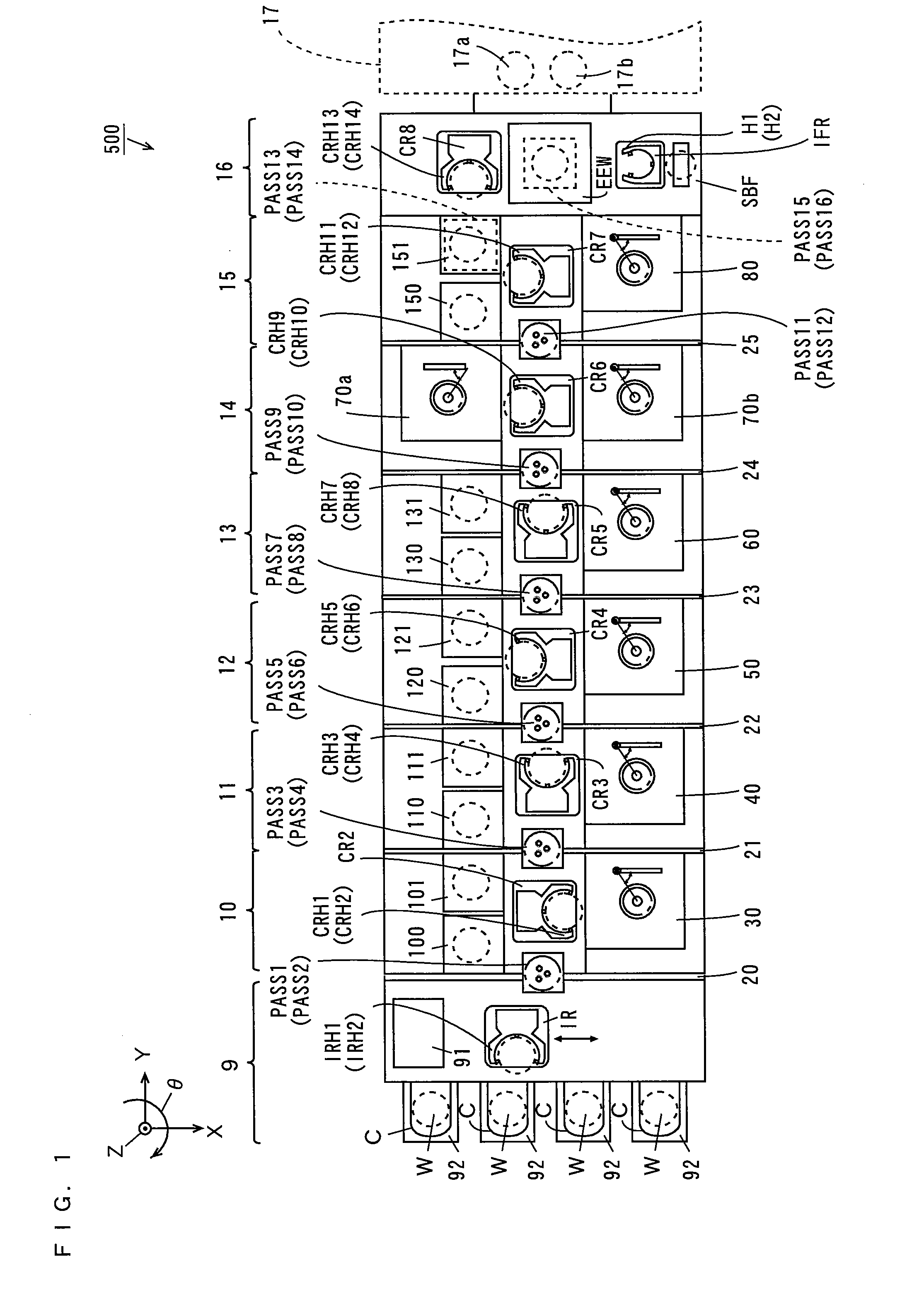
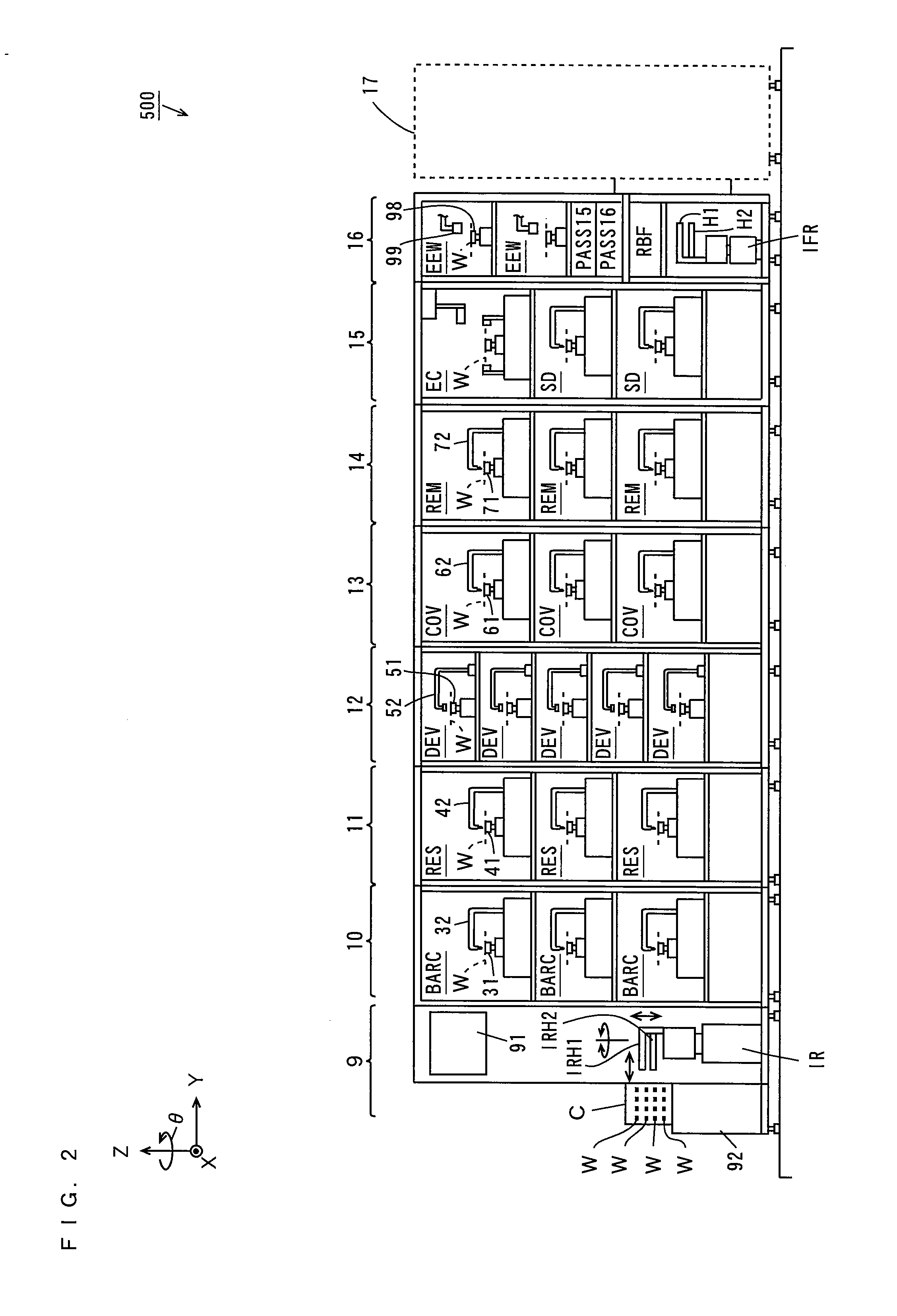
[0096] A substrate processing apparatus according to an embodiment of the present invention will be described with reference to the drawings. In the following description, a substrate refers to a semiconductor substrate, a substrate for a liquid crystal display, a substrate for a plasma display, a glass substrate for a photomask, a substrate for an optical disk, a substrate for a magnetic disk, a substrate for a magneto-optical disk, a substrate for a photomask, or the like, and the substrate contains silicon (Si).

[0097] The following drawings are accompanied by arrows that respectively indicate X, Y, and Z directions perpendicular to one another for clarity of a positional relationship. The X and Y directions are perpendicular to each other within a horizontal plane, and the Z direction corresponds to a vertical direction. In each of the directions, the direction of the arrow is defined as a +direction, and the opposite direction is defined as a −direction. A rotation direction ce...


PUM

PropertyMeasurementUnit
distanceaaaaaaaaaa
speedsaaaaaaaaaa
photosensitiveaaaaaaaaaa

Abstract

A substrate processing apparatus comprises an indexer block, an anti-reflection film processing block, a resist film processing block, a development processing block, a resist cover film processing block, a resist cover film removal block, a cleaning / drying processing block, and an interface block. An exposure device is arranged adjacent to the interface block in the substrate processing apparatus. The exposure device subjects a substrate to exposure processing by means of an immersion method. In the edge cleaning unit in the cleaning / drying processing block, a blush abuts against an end of the rotating substrate, so that the edge of the substrate before the exposure processing is cleaned. At this time, the position where the substrate is cleaned is corrected.

Description

BACKGROUND OF THE INVENTION [0001] 1. Field of the Invention [0002] The present invention relates to a substrate processing apparatus that subjects substrates to processing. [0003] 2. Description of the Background Art [0004] Substrate processing apparatuses are used to subject various types of substrates such as semiconductor substrates, substrates for liquid crystal displays, plasma displays, optical disks, magnetic disks, magneto-optical disks, and photomasks, and other substrates to various types of processing. [0005] Such a substrate processing apparatus generally subjects a single substrate to a plurality of different types of processing successively. The substrate processing apparatus as described in JP 2003-324139 A comprises an indexer block, an anti-reflection film processing block, a resist film processing block, a development processing block, and an interface block. An exposure device is arranged adjacent to the interface block as an external device separate from the sub...

Claims


Application Information

Patent Timeline
Patent Type & Authority Applications(United States)
IPC IPC(8): G03C5/00
CPCG03F7/168G03F7/7075G03F7/70916G03F7/70925Y10S134/902G11B5/8404G11B7/261H01L21/67051H01L21/67225G03F7/70991
Inventor KANEYAMA, KOJIKANAOKA, MASASHIMIYAGI, TADASHISHIGEMORI, KAZUHITOYASUDA, SHUICHIHAMADA, TETSUYA
Owner SOKUDO CO LTD
Why Eureka
Try Eureka