
Method for manufacturing single crystal semiconductor

a single crystal semiconductor and manufacturing method technology, applied in the direction of polycrystalline material growth, crystal growth process, polycrystalline material growth, etc., can solve the problems of degrading planarity and minute irregularities produced by concentration variations, and achieve the reduction of variation in hardness across the semiconductor wafer surface, the effect of controlling the fluctuation of pulling up speed and lowering the concentration of impurities

Active Publication Date: 2007-08-23
SUMCO TECHXIV
View PDF4 Cites 5 Cited by
  • Summary
  • Abstract
  • Description
  • Claims
  • Application Information

AI Technical Summary

Benefits of technology

[0012] The present invention has been made in view of such a situation, and the purpose thereof is to provide a method for manufacturing a single crystal semiconductor that, in the process of pulling up the single crystal semiconductor from the melt for growing it, incorporates an impurity more uniformly into the single crystal semiconductor, reducing the variation in impurity concentration across the semiconductor wafer surface, and thus, improving the planarity of the wafer.
[0035] However, according to the present invention, by controlling the fluctuation in pulling-up speed regardless of the magnitude of the impurity concentration, the effect that the variation in impurity concentration across the silicon wafer surface can be reduced is obtained, thus the present invention can be implemented without being limited to the high concentrations as specified by the fifth invention and the sixth invention.

Problems solved by technology

Likewise, if the silicon wafer is etched in the etching process, the variation in concentration produces minute irregularities.
The minute irregularities thus formed may degrade the planarity.

Method used


Image

  • Method for manufacturing single crystal semiconductor
  • Method for manufacturing single crystal semiconductor
  • Method for manufacturing single crystal semiconductor

Examples


Embodiment Construction

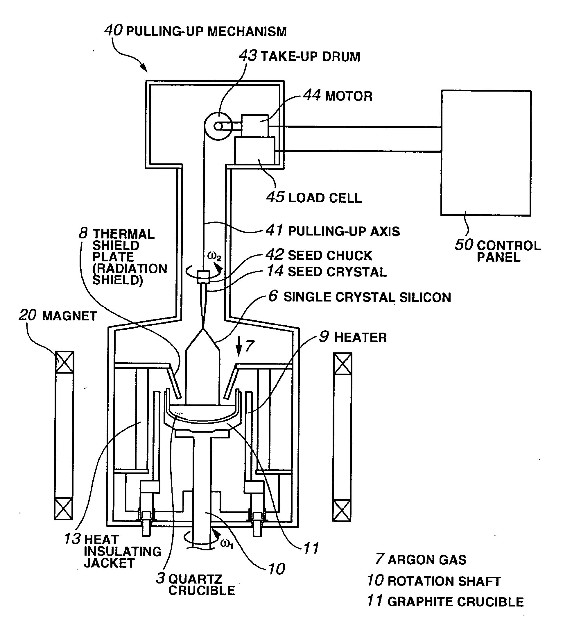
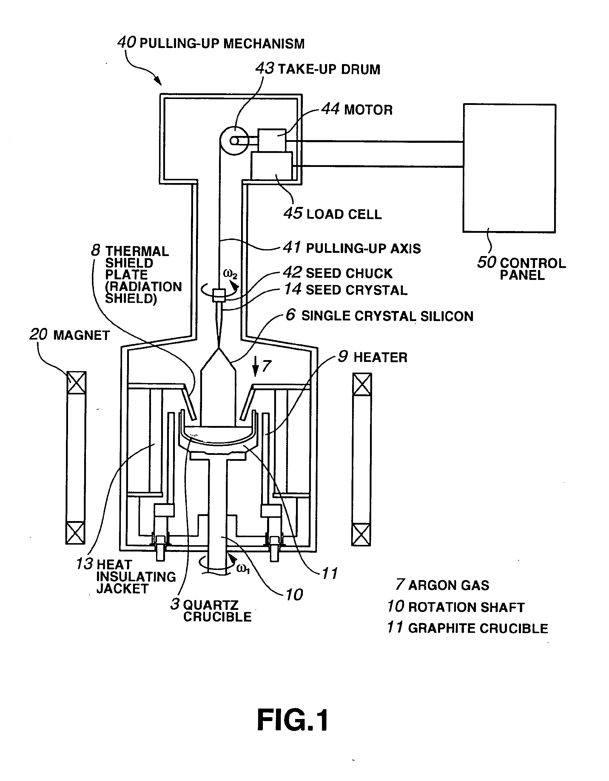
[0043] Hereinbelow, an apparatus of the embodiment will be described with reference to the drawings.

[0044]FIG. 1 is a schematic sectional view of the embodiment, illustrating the configuration thereof

[0045] As shown in FIG. 1, a single crystal pulling-up device 1 of the embodiment comprises a CZ furnace (chamber) 2 as a single crystal pulling-up vessel. The single crystal pulling-up device 1 in FIG. 1 is an apparatus, for example, suited for manufacturing a single crystal silicon ingot 6 having a diameter of 200 mm to 300 mm.

[0046] In the CZ furnace 2, a quartz crucible 3 for melting a raw material of polysilicon and accommodating it as a melt 5 is provided. For pulling up a single crystal silicon having a diameter of 300 mm, a polysilicon material weighing 300 kg or so is charged in the quartz crucible 3. The outside of the quartz crucible 3 is covered with a graphite crucible 11. At the side of the quartz crucible 3 outside thereof, a cylindrical heater 9 for heating the polysi...


PUM

PropertyMeasurementUnit
speedaaaaaaaaaa
magnetic fieldaaaaaaaaaa
speed fluctuationaaaaaaaaaa

Abstract

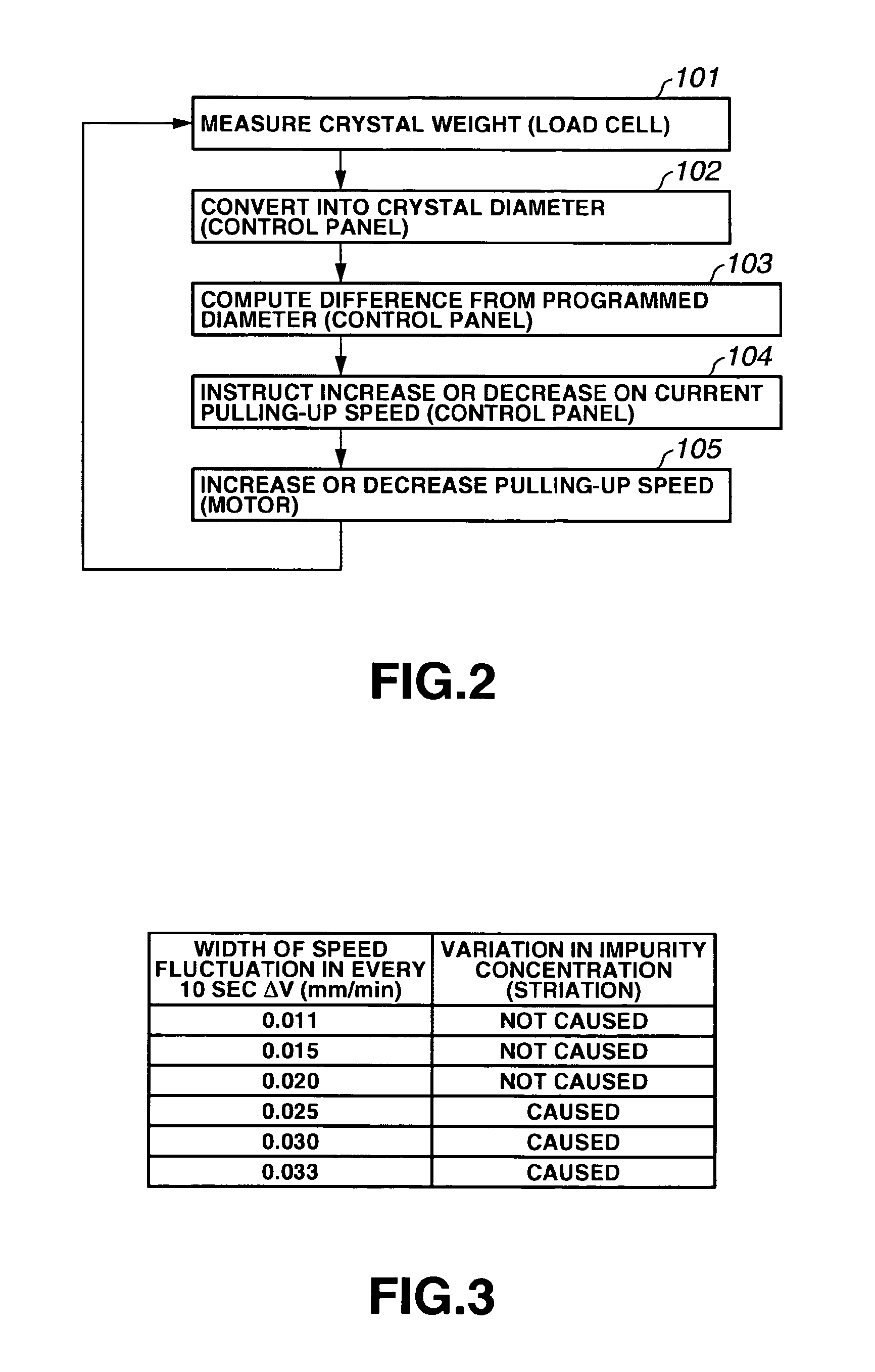
A method for manufacturing a single crystal semiconductor, in which, in a process of pulling up the single crystal semiconductor from melt for growing it, an impurity is incorporated more uniformly into the single crystal semiconductor so that a variation in impurity concentration across the semiconductor wafer surface can be reduced, and thus, the planarity of the wafer can be improved. In the process of pulling-up the single crystal semiconductor (6), fluctuation in a pulling-up speed is controlled, whereby the variation in concentration of the impurity in the single crystal semiconductor (6) is reduced. Especially, a width of speed fluctuation (ΔV) in 10 seconds is adjusted to less than 0.025 mm / min. Furthermore, in carrying out the control for adjusting the pulling-up speed such that a diameter of the single crystal semiconductor (6) becomes a desired diameter, a magnetic field having strength of 1,500 gauss or more is applied to the melt (5).

Description

TECHNICAL FIELD [0001] The present invention relates to a method for manufacturing a single crystal semiconductor, such as single crystal silicon, using the CZ method (Czochralski Method), and a method for manufacturing a single crystal semiconductor such that semiconductor wafers having a high planarity can be acquired. BACKGROUND ART [0002] As one of the manufacturing methods for single crystal silicon, the CZ method is available. [0003] The single crystal silicon (ingot) which is grown and pulled up by the CZ method is sliced, polished, and etched to be provided as a silicon wafer for manufacturing semiconductor devices. [0004] More specifically, an impurity, such as boron B or the like, is added into melt in order to provide a desired resistivity for the silicon wafer before the single crystal silicon is pulled up from the melt. [0005] Herein, in the process of pulling-up the single crystal silicon for growing it, the impurity is not uniformly incorporated. Therefore, when a sil...

Claims


Application Information

Patent Timeline
Patent Type & Authority Applications(United States)
IPC IPC(8): C30B11/00C30B15/20C30B15/30
CPCC30B15/20C30B15/305Y10T117/1056Y10T117/1068C30B29/06
Inventor INAGAKI, HIROSHIHONMA, MASANORIKAWASHIMA, SHIGEKISHIBATA, MASAHIRO
Owner SUMCO TECHXIV
Learn More