Electroless plating apparatus and plating solution

Inactive Publication Date: 2007-08-23
EBARA CORP
View PDF2 Cites 18 Cited by
  • Summary
  • Abstract
  • Description
  • Claims
  • Application Information

AI Technical Summary

Benefits of technology

[0039] It becomes possible with the present invention to reduce a stress on a plating solution, which is produced upon a change in the temperature of the plating solution due to the presence of components having different temperature dependencies of pH

Problems solved by technology

When an electroless plating process for forming a protective film selectively on the exposed surfaces of embedded interconnects is added to a manufacturing line of a semiconductor device, the cost of the process is desirably as low as possible.
The use of a high temperature and a high pH, however, makes the plating solution uns

Method used


Image

  • Electroless plating apparatus and plating solution
  • Electroless plating apparatus and plating solution
  • Electroless plating apparatus and plating solution

Examples


Example

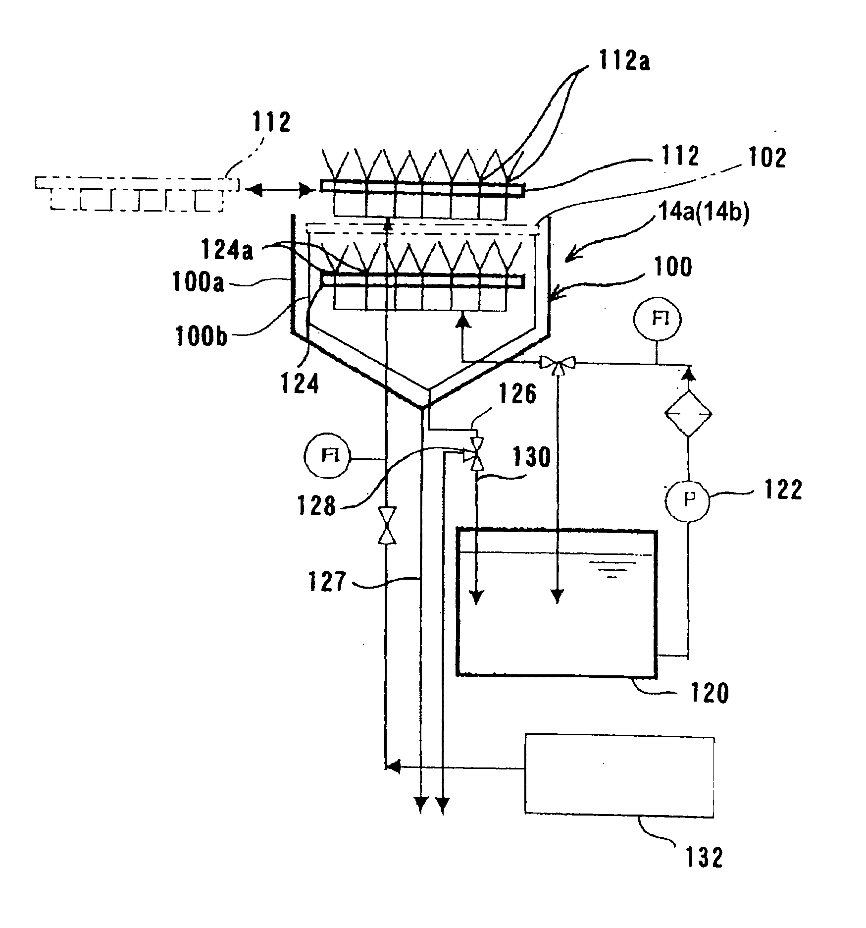
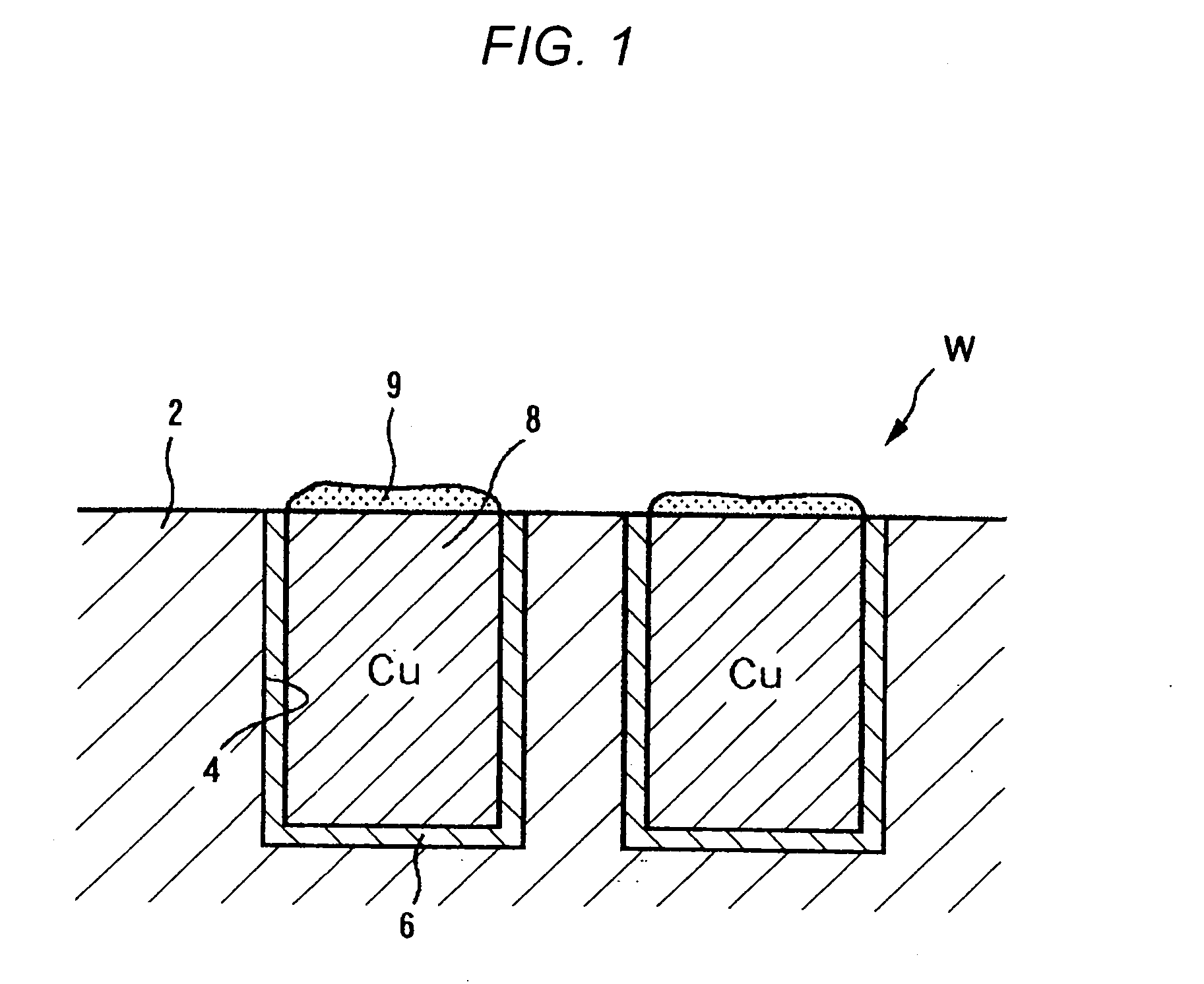
[0061] An electroless plating apparatus according to an embodiment of the present invention will now be described with reference to the drawings. The following description illustrates a case of selectively covering exposed surfaces of interconnects 8 with a protective film (cap material) 9 of a CoWP alloy to protect interconnects 8, as shown in FIG. 1. The present invention may also be adapted to cover a surface of copper, silver or the like with a metal film by depositing the metal film (plated film) of a Co alloy, a Ni alloy or the like.

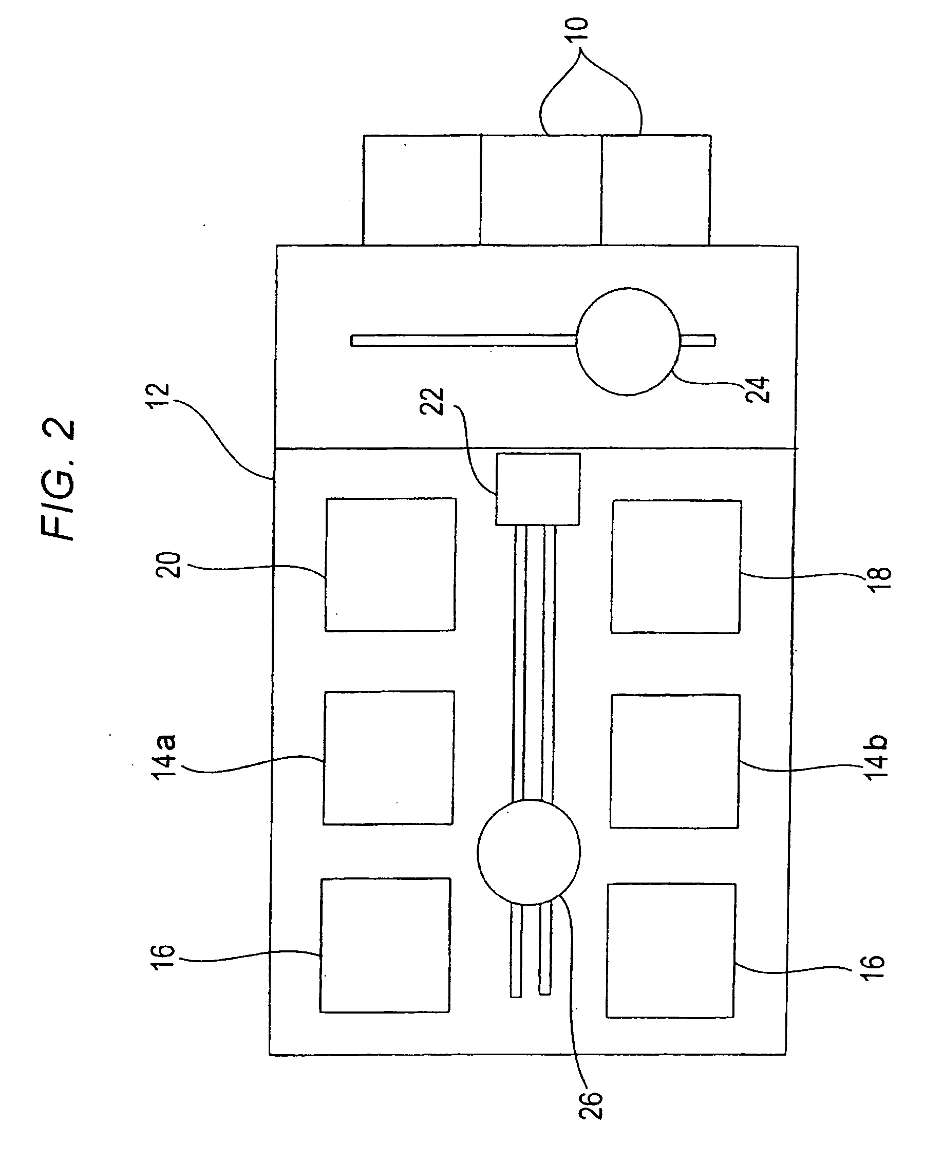
[0062]FIG. 2 is a layout plan view of a substrate processing apparatus incorporating an electroless plating apparatus according to an embodiment of the present invention. As shown in FIG. 2, the substrate processing apparatus is provided with loading / unloading units 10 each for mounting substrate cassette which accommodate a number of substrates W, such as semiconductor wafers, having interconnects 8 of, e.g., copper on the surfaces. Inside of a r...


PUM

PropertyMeasurementUnit
Temperatureaaaaaaaaaa
Densityaaaaaaaaaa
Acidityaaaaaaaaaa

Abstract

An electroless plating apparatus can suppress a change in quality of a plating solution and form a plated film without loss of its properties and reliability. The electroless plating apparatus includes a plating solution circulation system having a plating solution supply pipe for supplying a plating solution in a plating solution reservoir tank to a plating tank and a plating solution recovery pipe for returning the plating solution in the plating tank to the plating solution reservoir tank, and a heat retention section for preventing lowering of the temperature of the plating solution in the entire plating solution circulation system.

Description

BACKGROUND OF THE INVENTION [0001] 1. Field of the Invention [0002] The present invention relates to an electroless plating apparatus and a plating solution, and more particularly to an electroless plating apparatus used for forming, on bottom surfaces and side surfaces or exposed surfaces of embedded interconnects which have been formed by embedding an interconnect material (conductive material), such as copper or silver, into fine interconnect recesses provided in a surface of a substrate such as a semiconductor wafer, a conductive film having a function to prevent thermal diffusion of the interconnect material into an interlevel dielectric layer or a function to improve adhesiveness between the interconnects and an interlevel dielectric layer, or a protective film, such as magnetic film, covering interconnects, and a plating solution. [0003] 2. Description of the Related Art [0004] As an interconnect formation process for semiconductor devices, there is getting employed a process...

Claims


Application Information

Patent Timeline
IPC IPC(8): B05C3/00
CPCC23C18/1619H01L21/76849H01L21/288C23C18/50
Inventor SAIJO, YASUHIKOKOBA, TAKASHITSUJINO, JUNICHIRO
Owner EBARA CORP
Why Eureka
Try Eureka