Shielded gate trench (SGT) MOSFET devices and manufacturing processes

Active Publication Date: 2007-08-23
ALPHA & OMEGA SEMICON LTD
View PDF4 Cites 104 Cited by
  • Summary
  • Abstract
  • Description
  • Claims
  • Application Information

AI Technical Summary

Benefits of technology

[0010]It is therefore an aspect of the present invention to provide a new and improved semiconductor power device implemented with the shielded gate trench (SGT) structure that has the bottom-shielding electrode provided with improved connection more directly to the source voltage. Specifically, a macro-cell layout approach is disclosed. In the macro-cell,

Problems solved by technology

Conventional technologies for reducing the gate to drain capacitance Cgd in a power semiconductor device are still confronted with technical limitations and difficulties.
The above patented-disclosures including tra

Method used


Image

  • Shielded gate trench (SGT) MOSFET devices and manufacturing processes
  • Shielded gate trench (SGT) MOSFET devices and manufacturing processes
  • Shielded gate trench (SGT) MOSFET devices and manufacturing processes

Examples


Embodiment Construction

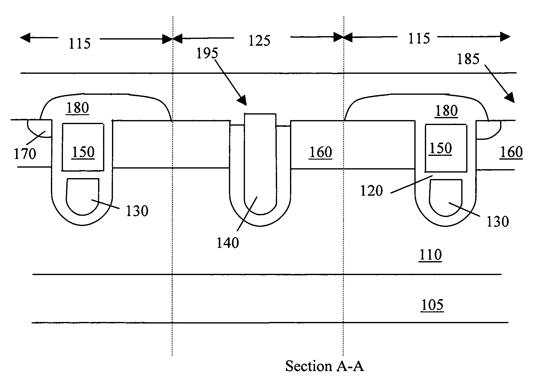
[0020]Referring to FIGS. 2A to 2D for a top view and three cross sectional views respectively of a trenched MOSFET device 100 of this invention. As shown in FIG. 2B, the trenched MOSFET device 100 is supported on a substrate 105 formed with an epitaxial layer 110. The trenched MOSFET device 100 includes a shielded gate trench (SGT) structure. The SGT structure includes a bottom-shielding electrode 130 insulated from and disposed below a trenched gate 150. The bottom SGT structure 130 filled with a polysilicon therein is provided to shield the trenched gate 150 from the drain disposed below trench bottom. The bottom SGT structure 130 is insulated from the drain region by a dielectric layer 113. An insulation layer 120 separated the bottom-shielding electrode 130 from the trenched gate 150. The trenched gate 150 includes polysilicon filling in a trench surrounded with a gate insulation layer 155 covering the trench walls. A body region 160 that is doped with a dopant of second conduct...


PUM


Abstract

This invention discloses a semiconductor power device that includes a plurality of power transistor cells surrounded by a trench opened in a semiconductor substrate. At least one of the cells constituting an active cell has a source region disposed next to a trenched gate electrically connecting to a gate pad and surrounding the cell. The trenched gate further has a bottom-shielding electrode filled with a gate material disposed below and insulated from the trenched gate. At least one of the cells constituting a source-contacting cell surrounded by the trench with a portion functioning as a source connecting trench is filled with the gate material for electrically connecting between the bottom-shielding electrode and a source metal disposed directly on top of the source connecting trench. The semiconductor power device further includes an insulation protective layer disposed on top of the semiconductor power device having a plurality of source openings on top of the source region and the source connecting trench provided for electrically connecting to the source metal and at least a gate opening provided for electrically connecting the gate pad to the trenched gate.

Description

BACKGROUND OF THE INVENTION[0001]1. Field of the Invention[0002]The invention relates generally to the semiconductor power devices. More particularly, this invention relates to an improved and novel manufacturing process and device configuration for providing the MOSFET device with shielded trench gates (STG) for providing high frequency power switching device.[0003]2. Description of the Prior Art[0004]Conventional technologies for reducing the gate to drain capacitance Cgd in a power semiconductor device are still confronted with technical limitations and difficulties. As there are growing demands for high frequency switch power devices, an urgent need exists to provide effective solutions to achieve the purpose of resolving these technical difficulties and limitations. For power transistors including MOSFET and IGBT, a new device configuration and manufacturing process are necessary to reduce the speed-limiting capacitance between the gate and the drain of these switching power de...

Claims


Application Information

Patent Timeline
IPC IPC(8): H01L29/94H01L21/336
CPCH01L29/0696H01L29/407H01L29/7813H01L29/7811H01L29/66734
Inventor BHALLA, ANUPLUI, SIK K.
Owner ALPHA & OMEGA SEMICON LTD
Why Eureka
Try Eureka