Stacked semiconductor memory device and control method thereof

Active Publication Date: 2007-08-23
MICRON TECH INC
View PDF3 Cites 51 Cited by
  • Summary
  • Abstract
  • Description
  • Claims
  • Application Information

AI Technical Summary

Benefits of technology

[0018]While data is successively transferred via the predetermined data through electrode, it is preferable that a parity of the data be transferred via a data through electrode different from the predetermined data

Problems solved by technology

However, the miniaturization of memory cells is physically limited, and the increase in chip size leads to a reduction of yield and impairs an increase of operating speed.
For this reason, a simultaneous data transfer from the plurality of memory arrays (or to the plurality of memory arrays) by using one through electrode is not possible.
Thus, when the reaction rate (1 to 2 ns) of the through electrode, an output retaining period (1 to 2 ns) of the data, and the like are added, the limit of a data transfer cycle during which one through electrode is used is approximately 15 to 20 ns, a

Method used


Image

  • Stacked semiconductor memory device and control method thereof
  • Stacked semiconductor memory device and control method thereof
  • Stacked semiconductor memory device and control method thereof

Examples


first embodiment

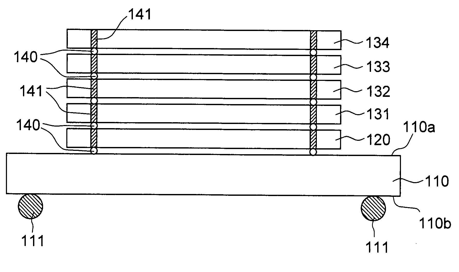
[0033]FIG. 1 is a schematic cross-sectional view showing a structure of a stacked semiconductor memory device according to the present invention.

[0034]As shown in FIG. 1, the stacked semiconductor memory device according to the first embodiment includes an interposer substrate 110, an interface chip 120 mounted on one surface 110a of the interposer substrate 110, and a plurality (four, for example) of core chips 131 to 134 stacked on the interface chip 120. Thus, the stacked semiconductor memory device according to the first embodiment has a structure in which a plurality of semiconductor chips including the plurality of core chips 131 to 134 are stacked.

[0035]Transmission of a signal to and from an external circuit is performed via external terminals 111 arranged on the other surface 110b of the interposer substrate 110. Transmission of a signal between the interface chip 120 and the core chips 131 to 134 is performed via internal terminals 140 and through electrodes 141. In a stac...

second embodiment

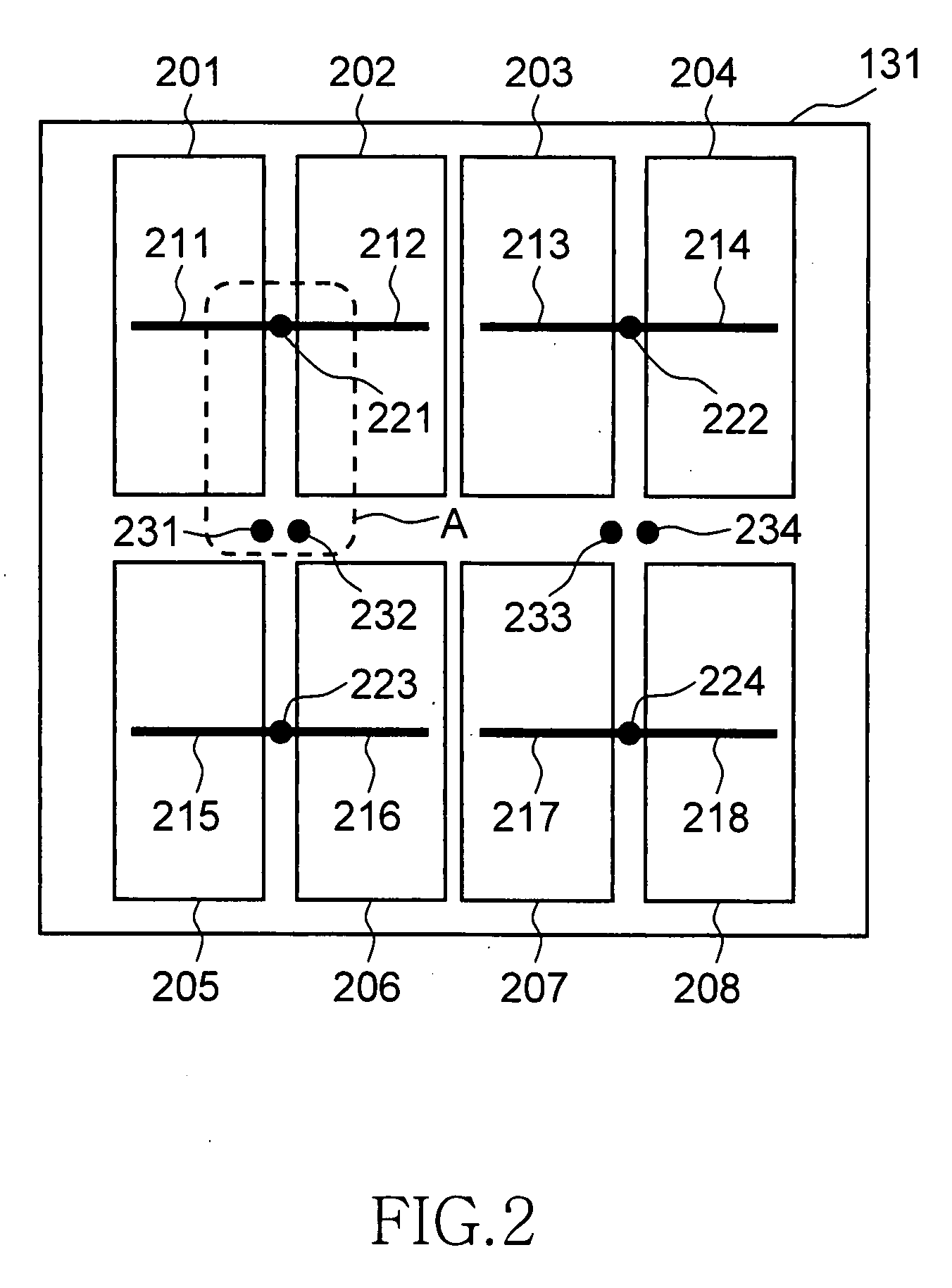
[0060]FIG. 6 is a circuit diagram showing a structure of principal parts of a stacked semiconductor memory device and corresponds to an area A shown in FIG. 2. The basic configuration of the entire device is the same as those of FIGS. 1 and 2.

[0061]As shown in FIG. 6, in the second embodiment, the control nodes 241a and 242a of the switch circuits 241 and 242 are supplied with output signals of AND circuits 261 and 262, respectively. One input node of the AND circuit 261 is supplied with an activation signal S11, and one input node of the AND circuit 262 is supplied with an activation signal S12. The activation signal S11 is a signal that corresponds to the memory array 201 included in each of the core chips 131 to 134. When the activation signal S11 is active (high level), the memory array 201 included in each of the core chips 131 to 134 is almost simultaneously activated. On the other hand, the activation signal S12 is a signal that corresponds to the memory array 202 included i...

third embodiment

[0073]Principal parts of a stacked semiconductor memory device have the same circuit configuration as that shown in FIG. 2.

[0074]FIG. 9 is a timing chart for explaining an operation of the stacked semiconductor memory device according to the third embodiment.

[0075]Firstly, before a time t30, the activation signal S1 is inactive (low level). Accordingly, the memory arrays 201 and 202 (memory arrays 201 and 202 included in the core chip 131) that correspond to the activation signal S1 are not activated. Before the time t30, the activation signal S2 is also inactive (low level). As explained above, the activation signal S2 is a signal for activating the memory arrays 201 and 202 included in the core chip 132. Accordingly, the memory arrays 201 and 202 included in the core chip 132 are not activated either. Before the time t30, the selection signals SL and SR are invalid (Don't Care).

[0076]When there is an access request from outside, the activation signal S1 becomes active (high level...


PUM


Abstract

A stacked semiconductor memory device includes an interface chip and a plurality of core chips, in which the interface chip and the plurality of core chips are stacked. The core chips are mutually connected by a plurality of data through electrodes. The core chips each include a plurality of memory arrays. In response to an access request, the plurality of memory arrays corresponding to a predetermined data through electrode are activated, and the plurality of activated memory arrays and the predetermined data through electrode are sequentially connected. Thereby, even though it requires approximately ten-odd ns for transferring the first data, similarly to the conventional case, it is possible to transfer the subsequent data at high speed determined by the reaction rate (1 to 2 ns) of the through electrode. As a result, it becomes possible to increase a bandwidth while suppressing the number of through electrodes.

Description

TECHNICAL FIELD[0001]The present invention relates to a stacked semiconductor memory device and a control method thereof. More particularly, the invention relates to a stacked semiconductor memory device in which data or the like are sent and received via a plurality of through electrodes arranged on semiconductor chips, and also to a control method thereof.BACKGROUND OF THE INVENTION[0002]In recent years, the storage capacity of semiconductor memory devices, represented by a DRAM (Dynamic Random Access Memory), has increased. It is increasingly demanded that these devices can operate at higher speeds. The increase in storage capacity has been achieved by making memory cells smaller and by increasing the chip size. However, the miniaturization of memory cells is physically limited, and the increase in chip size leads to a reduction of yield and impairs an increase of operating speed.[0003]To solve these problems fundamentally, there has been proposed a method such that a core unit h...

Claims


Application Information

Patent Timeline
IPC IPC(8): H01L23/52H01L23/48H01L29/40
CPCH01L25/0657H01L2224/16225H01L2225/06513H01L2924/15311H01L2225/06527H01L2225/06541H01L2225/06586H01L2225/06517H01L2224/16145
Inventor IKEDA, HIROAKISHIBATA, KAYOKO
Owner MICRON TECH INC
Why Eureka
Try Eureka