Electronic device with uniform-resistance fan-out blocks

a technology of uniform resistance and fan-out blocks, which is applied in the field of thin film transistor liquid crystal display panels (tftlcd) panels, can solve problems such as downgrading the entire image quality, and achieve the effect of uniform resistan

Active Publication Date: 2007-08-23
AU OPTRONICS CORP
View PDF4 Cites 28 Cited by
  • Summary
  • Abstract
  • Description
  • Claims
  • Application Information

AI Technical Summary

Benefits of technology

[0008]It is another object of the present invention to provide an electronic device, such as an LCD panel, and a manufacturing method therefor such that the adjacent interconnecting leads of two adjacent fan-out blocks have uniform resistance to ensure the operation quality.

Problems solved by technology

Such difference of resistances may impact the time delay and quality of control signals from external driving ICs and may thus downgrade the entire image quality.

Method used


Image

  • Electronic device with uniform-resistance fan-out blocks
  • Electronic device with uniform-resistance fan-out blocks
  • Electronic device with uniform-resistance fan-out blocks

Examples


Embodiment Construction

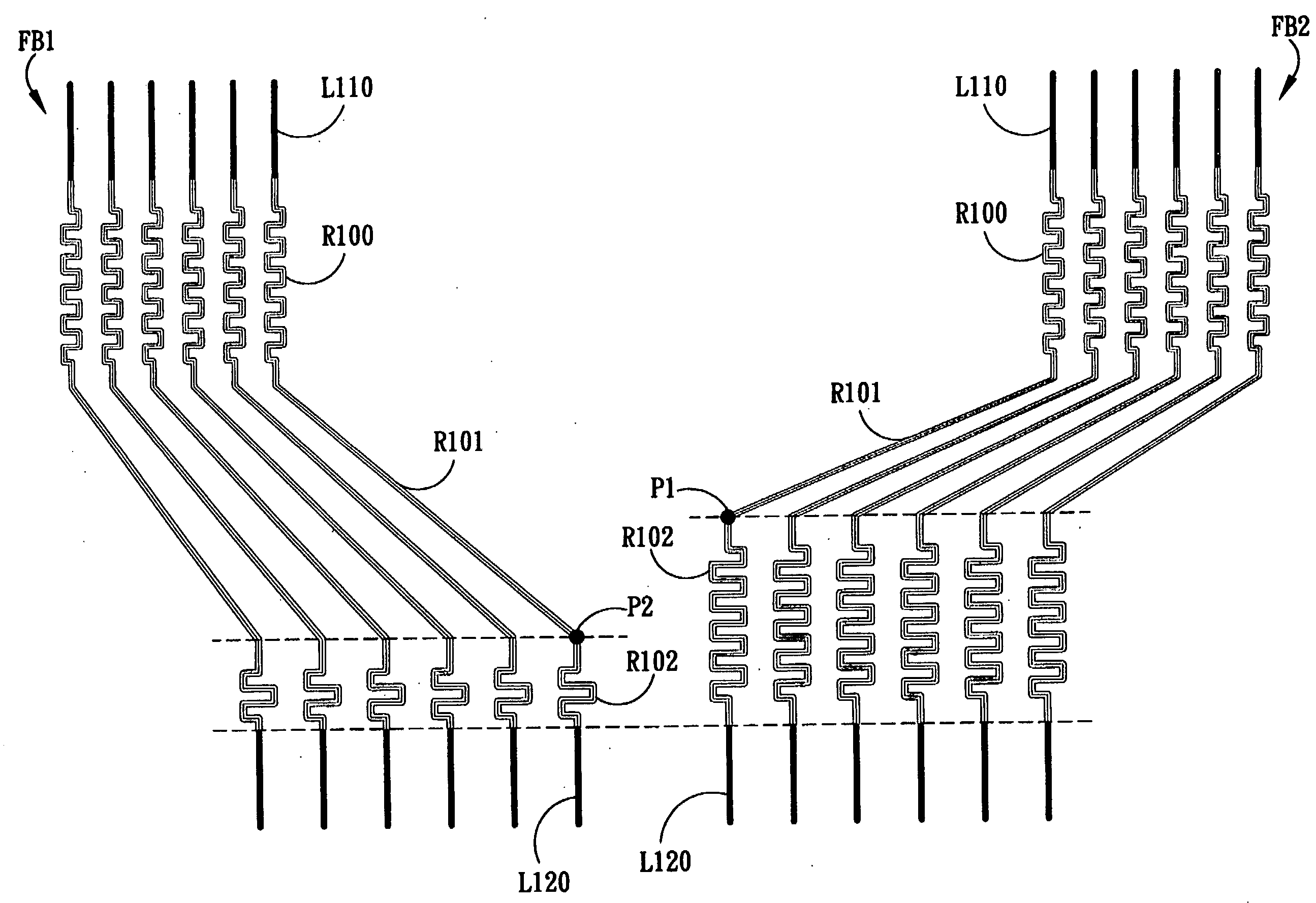
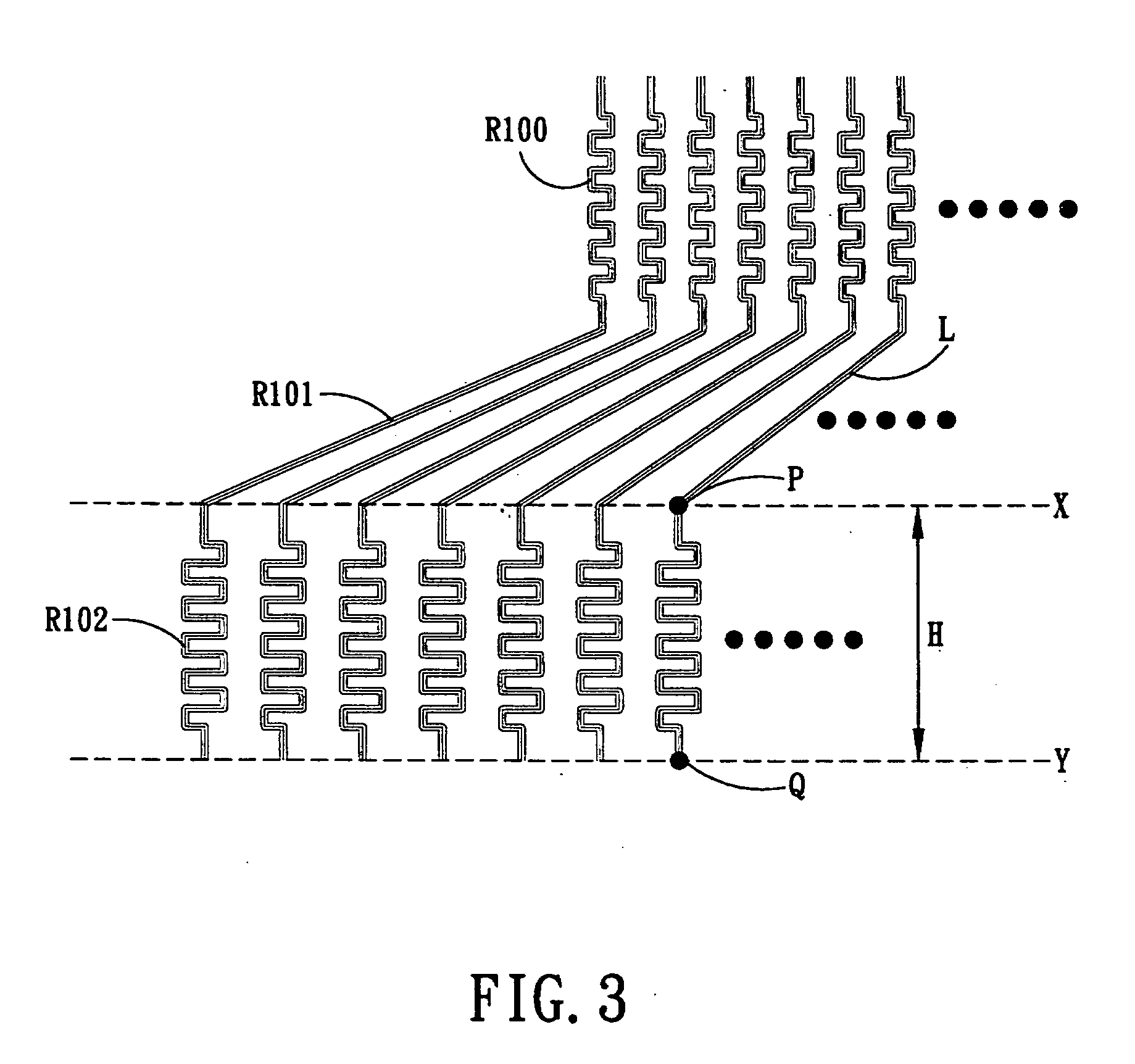
[0018]Except fan-out blocks, the structure of elements of the LCD panel disclosed in the embodiments of the present invention is identical with that shown in FIG. 1. The description about the structure of a general LCD panel shown in FIG. 1 is thus applicable for the present invention. FIG. 3 shows an embodiment of the layout of a fan-out block in accordance with the present invention, which includes multiple interconnecting leads L, each interconnecting lead L at least including three portions: the first routing portion R100 coupled to bonding pads in bonding area 20 (FIG. 1) and electrically connected with external driving IC(s), the second routing portion R102 connected with data lines 12 or gate lines 14, and the intermediate portion R101 locating and connecting between the first routing portion R100 and the second routing portion R102. In contrast with the second routing portion R102, the first routing portion R100 has a smaller pitch between adjacent interconnecting leads. Ref...


PUM

PropertyMeasurementUnit
resistanceaaaaaaaaaa
angleaaaaaaaaaa
intersecting angleaaaaaaaaaa

Abstract

The present invention provides an electronic device and manufacturing method thereof. The interconnecting leads of adjacent fan-out blocks have different heights along boundary area, thereby making the resistance of the adjacent interconnecting leads uniform and ensuring the quality of the electronic device.

Description

BACKGROUND OF THE INVENTION[0001]1. Field of the Invention[0002]The present invention relates to an electronic device with uniform-resistance fan-out blocks, and more particularly, to a thin film transistor liquid crystal display (TFT-LCD) panel with uniform-resistance fan-out blocks.[0003]2. Description of the Prior Art[0004]FIG. 1 shows a substrate 1 of a typical active matrix thin film transistor LCD panel, which generally includes an active area 10. The active area 10 includes data lines 12 and gate lines 14 which collectively carry signals to control transistor switches (not shown in FIG. 1) so as to drive pixels constructing an image on the display panel. Alternately, data lines 12 and gate lines 14 will be referred to as control lines in this specification. The portion surrounding the active area 10 is the out-lead bonding (OLB) area 16 which contains some bonding areas 20. Each bonding area 20 includes multiple bonding pads to be coupled with external driving integrating cir...

Claims


Application Information

Patent Timeline
Patent Type & Authority Applications(United States)
IPC IPC(8): G02F1/1345
CPCG02F1/136286G02F1/1345
Inventor LEE, MING-CHINLAI, MING-SHENG
Owner AU OPTRONICS CORP
Why Eureka
Try Eureka