Semiconductor memory device

a memory device and semiconductor technology, applied in the field of semiconductor memory devices, can solve the problems of increasing the error rate with an increase in the number of data rewrite operations, and increasing the workload of the host devi

Inactive Publication Date: 2007-08-23
KK TOSHIBA
View PDF7 Cites 20 Cited by
  • Summary
  • Abstract
  • Description
  • Claims
  • Application Information

AI Technical Summary

Benefits of technology

[0018] in the encoding part, M+16 (M≦255−16=239) terms corresponding to 16 check bits and M data bits to be error-corrected are sel

Problems solved by technology

Electrically rewritable nonvolatile semiconductor memory devices include “flash” memories, which increase in error rate with an increase in number of data rewrite operations.
In particular, the quest

Method used


Image

  • Semiconductor memory device
  • Semiconductor memory device
  • Semiconductor memory device

Examples


Embodiment Construction

[0048] Some embodiments of this invention will be described with reference to the accompanying figures of the drawing below.

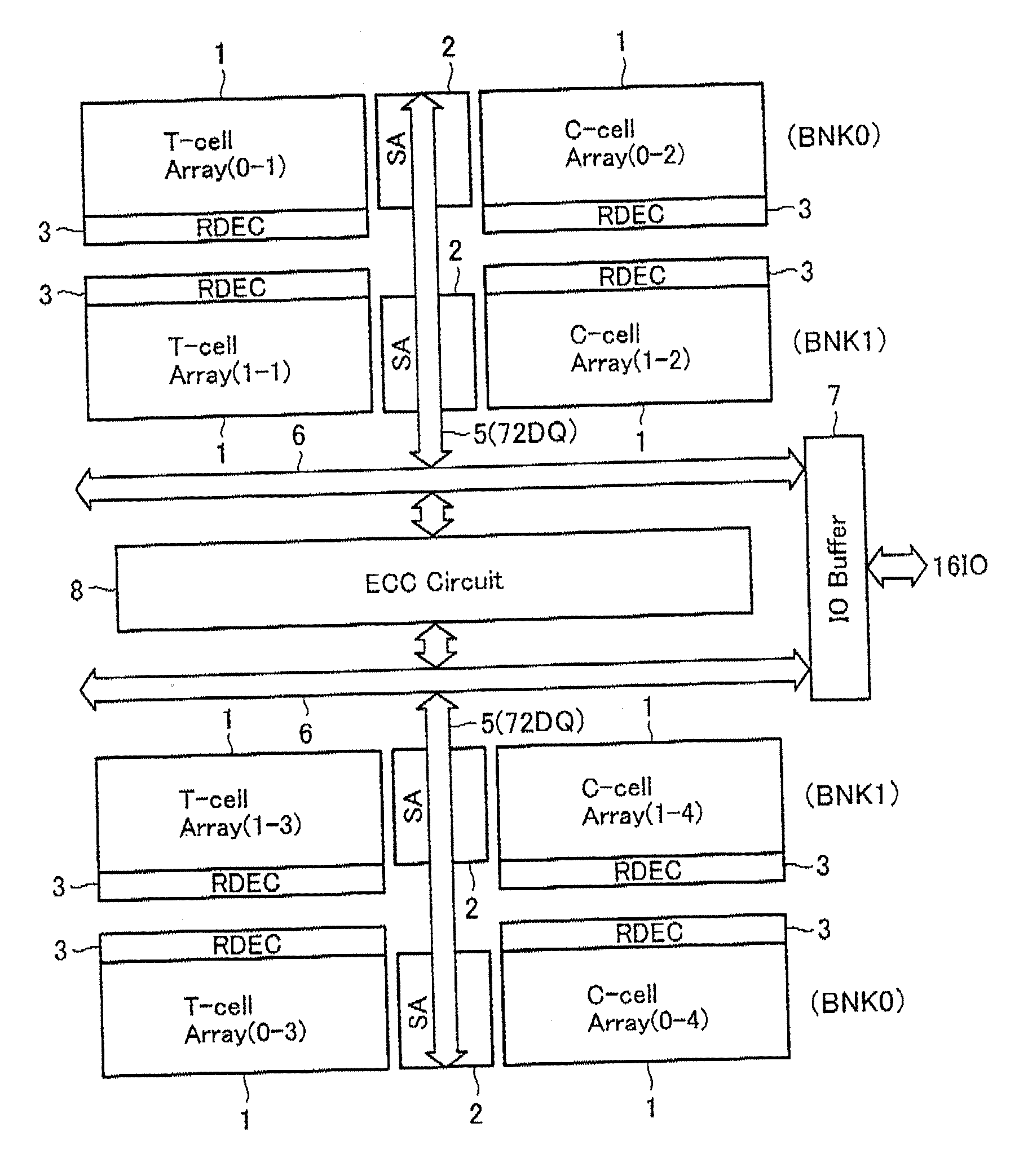
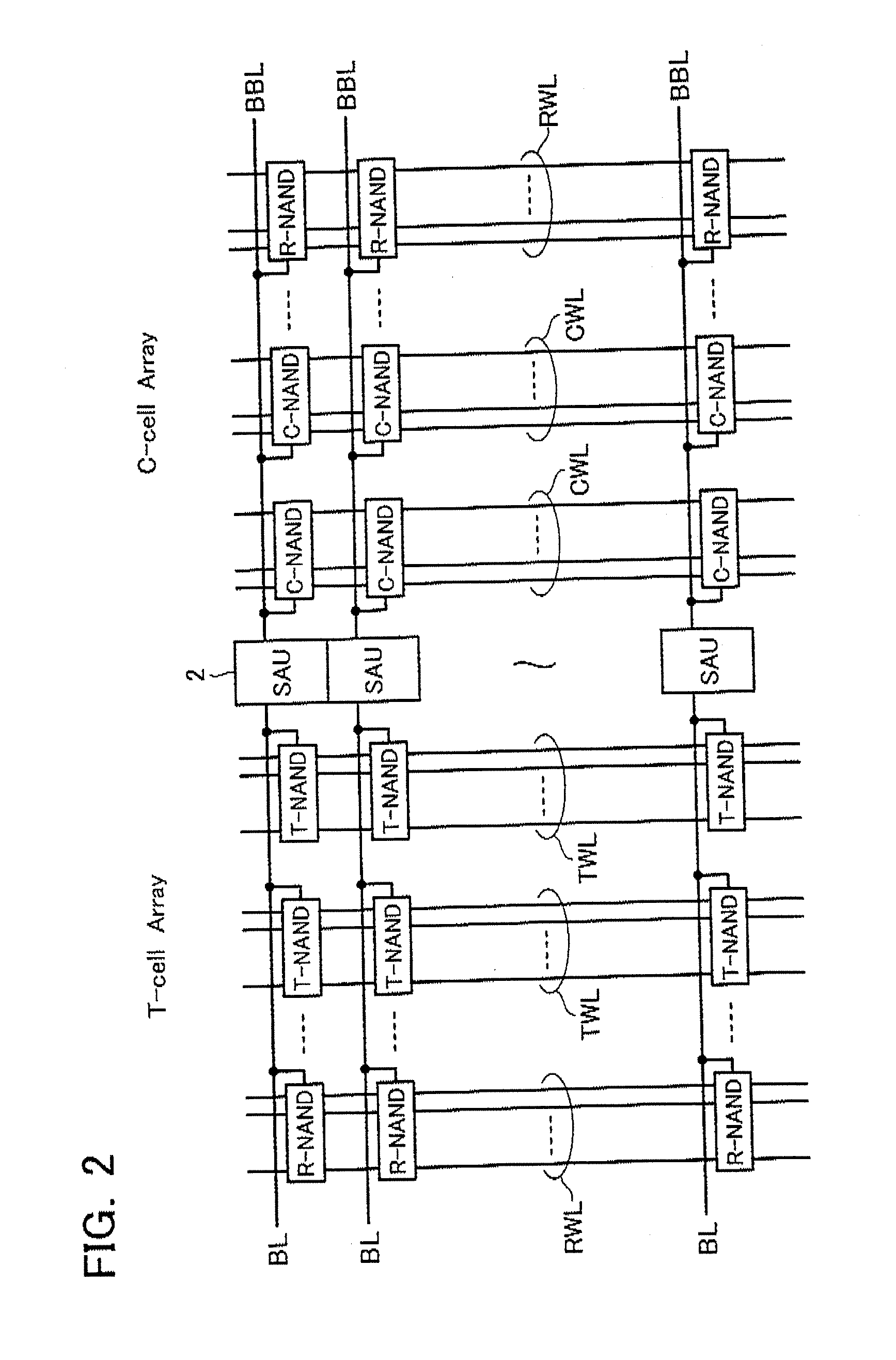
[0049] Referring to FIG. 1, there is illustrated a block diagram showing main parts of a flash memory embodying the invention. This flash memory includes a couple of banks BNK0 and BNK1. Bank BNK0 is formed of four separate memory cell arrays 1—i.e., T-cell array (0-1), C-cell array (0-2), T-cell array (0-3), and C-cell array (0-4). The other bank BNK1 also is formed of four cell arrays 1, i.e., T-cell array (1-1), C-cell array (1-2), T-cell array (1-3), and C-cell array (1-4).

[0050] Each cell array 1 is associated with a row decoder (RDEC) 3 for performing word-line selection. Sense amplifier (SA) circuits 2 are provided, each of which is commonly owned or “shared” by neighboring T-cell array and C-cell array. These T-cell and C-cell arrays have a plurality of information cells, T-cells and C-cells, respectively, each having at least one reference cell R-cel...


PUM


Abstract

A semiconductor memory device has a built-in error detection and correction system, wherein the error detection and correction system is formed to have a cyclic code, with which multiple error bits are correctable, and wherein the cyclic code is configured in such a manner that a certain number of degrees are selected as information bits from the entire degree of an information polynomial having degree numbers corresponding to an error-correctable maximal bit number, the certain number being a number of data bits which are simultaneously error-correctable in the memory device.

Description

CROSS-REFERENCE TO RELATED APPLICATION [0001] This application is based on and claims the benefit of priority from the prior Japanese Patent Application No. 2006-012648, filed on Jan. 20, 2006, the entire contents of which are incorporated herein by reference. BACKGROUND OF THE INVENTION [0002] 1. Field of the Invention [0003] This invention relates generally to a semiconductor memory device and, more particularly, to an on-chip error detection and correction system adaptable for use therein. [0004] 2. Description of the Related Art [0005] Electrically rewritable nonvolatile semiconductor memory devices include “flash” memories, which increase in error rate with an increase in number of data rewrite operations. In particular, the quest for larger storage capacity and further enhanced miniaturization results in an increase in error rate. In view of this, an attempt is made to mount or “embed” a built-in error correcting code (FCC) circuit on flash memory chips or, alternatively, in m...

Claims


Application Information

Patent Timeline
IPC IPC(8): H03M13/00
CPCH03M13/152H03M13/159H03M13/1545F24C15/2071F24C15/2085
Inventor TODA, HARUKI
Owner KK TOSHIBA
Why Eureka
Try Eureka