Calculation system for inverse masks

a technology of inverse masks and calculations, applied in the field of photolithography, can solve problems such as optical distortions, and achieve the effect of improving fidelity

Active Publication Date: 2007-08-23
SIEMENS PROD LIFECYCLE MANAGEMENT SOFTWARE INC
View PDF2 Cites 97 Cited by
  • Summary
  • Abstract
  • Description
  • Claims
  • Application Information

AI Technical Summary

Benefits of technology

[0006] To improve the fidelity by which a desired layout pattern can be printed on a wafer with a photolithographic imaging system, the present invention is a method and apparatus for calculating a mask or reticle layout pattern from a desired layout pattern. A computer system executes a sequence of instructions that cause the computer system to read all or a portion of a desired layout pattern and define a mask layout pattern as a number of pixel transmission characteristics. The computer system analyzes an objective function equation that relates the transmission characteristic of each pixel in the mask pattern to an image intensity on a wafer. In one embodiment, a maximum image intensity for points on a wafer is obtained from a maximum image intensity determined from a simulation of the image that would be formed using a test pattern of mask features. In one embodiment, the objective function also includes one or more penalty functions that enhance solutions meeting desired manufacturing restraints. Once the pixel transmission characteristics for the mask layout pattern are determined, the data are provided to a mask writer to fashion one or more corresponding masks for use in printing the desired layout pattern.

Problems solved by technology

As the components of the integrated circuit or other device to be created become ever smaller, optical distortions occur whereby a pattern of features defined on a mask or reticle do not match those that are printed on the wafer.

Method used


Image

  • Calculation system for inverse masks
  • Calculation system for inverse masks
  • Calculation system for inverse masks

Examples


Embodiment Construction

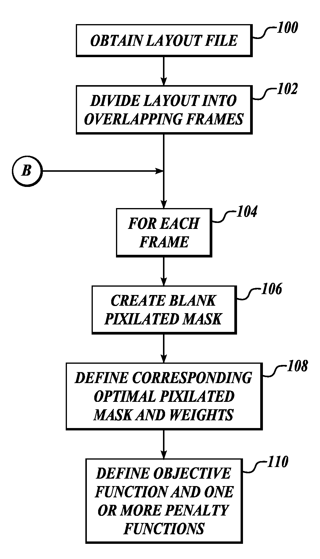
[0033] As will be explained in further detail below, the present invention is a method and apparatus for calculating a mask pattern that will print a desired layout or portion thereof on a wafer. FIG. 19 illustrates a representative computer system that can be used to calculate a mask layout pattern in accordance with one embodiment of the present invention. A computer system 50, including one or more programmable processors, receives a set of executable instructions on a computer-readable media 52 such as a CD, DVD, or from a communication link such as a wired or wireless communication network such as the Internet. The computer system 50 executes the instructions to read all or a portion of a desired layout file from a database 54 or other storage media. The computer system 50 then calculates data for a mask layout by dividing a mask layout into a number of discrete pixels. The computer system determines the transmission characteristic of each of the pixels so that the result on a ...


PUM


Abstract

A system for calculating mask data to create a desired layout pattern on a wafer reads all or a portion of a desired layout pattern. Mask data having pixels with transmission values is defined along with corresponding optimal mask data pixel transmission values. An objective function is defined that compares image intensities as would be generated on a wafer with an optimal image intensity at a point corresponding to a pixel. The objective function is minimized to determine the transmission values of the mask pixels that will reproduce the desired layout pattern on a wafer.

Description

CROSS-REFERENCE(S) TO RELATED APPLICATION(S) [0001] This application claims the benefit of U.S. Provisional Patent Application No. 60 / 792,476 filed Apr. 14, 2006, and is a continuation-in-part of U.S. patent application Ser. No. 11 / 364,802 filed Feb. 28, 2006, which in turn claims the benefit of U.S. Provisional Patent Application Ser. No. 60 / 657,260 filed Feb. 28, 2005; U.S. Provisional Patent Application Ser. No. 60 / 658,278, filed Mar. 2, 2005; and U.S. Provisional Patent Application Ser. No. 60 / 722,840 filed Sep. 30, 2005, which are all expressly incorporated by reference herein.FIELD OF THE INVENTION [0002] The present invention relates to photolithography, and in particular to methods of creating a semiconductor mask or reticle to print a desired layout pattern. BACKGROUND OF THE INVENTION [0003] With conventional photolithographic processing techniques, integrated circuits are created on a semiconductor wafer by exposing photosensitive materials on the wafer through a mask or ...

Claims


Application Information

Patent Timeline
Patent Type & Authority Applications(United States)
IPC IPC(8): G06F17/50
CPCG03F1/36G03F1/144
Inventor GRANIK, YURISAKAJIRI, KYOHEI
Owner SIEMENS PROD LIFECYCLE MANAGEMENT SOFTWARE INC
Why Eureka
Try Eureka