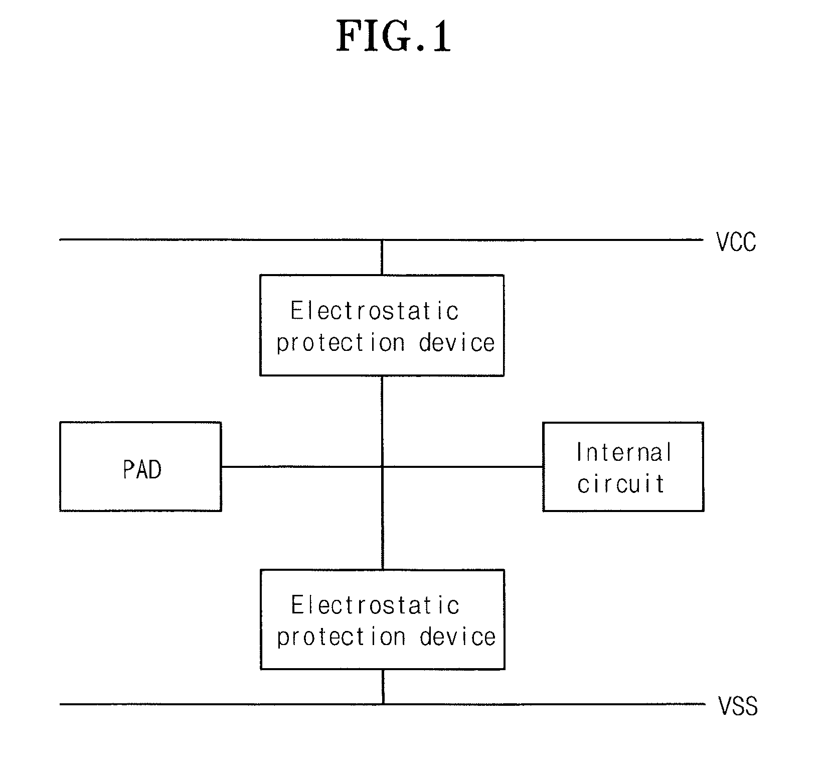
Electrostatic protection device for semiconductor circuit for decreasing input capacitance
a protection device and semiconductor technology, applied in the field of electrostatic protection devices for semiconductor circuits, can solve the problems of increasing the input capacitance of the semiconductor, significant and damage to the internal circuit of the semiconductor by the human body or machine, so as to minimize the input capacitance and achieve high-speed operation.
- Summary
- Abstract
- Description
- Claims
- Application Information
AI Technical Summary
Benefits of technology
Problems solved by technology
Method used
Image

Examples
Embodiment Construction
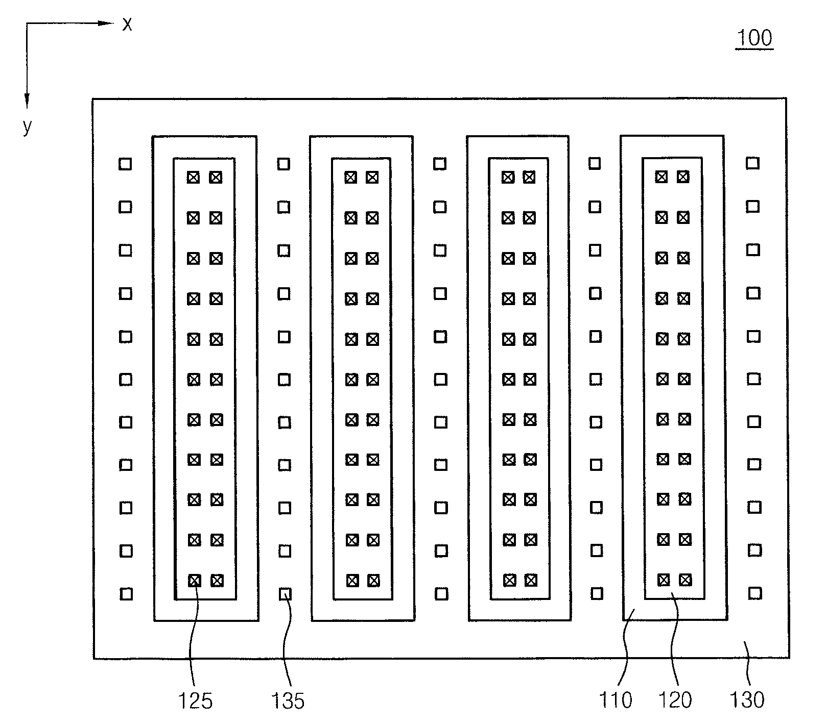
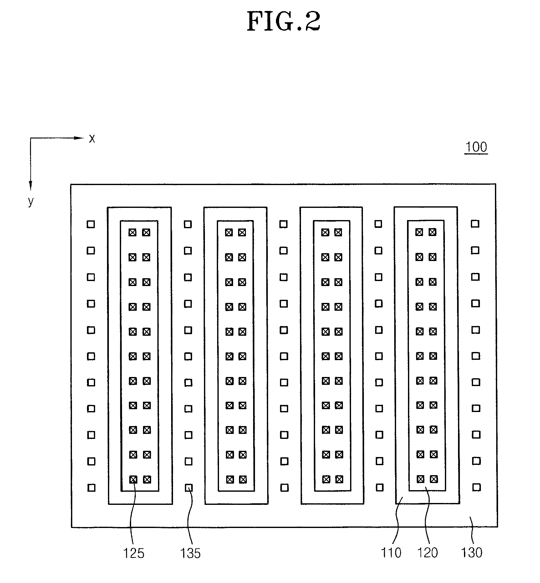
[0030]In an embodiment of the present invention, an electrostatic protection device is configured using a structure that maintains the perimeter as it is and reduces the junction area in comparison with the conventional art. In this case, since the perimeter is maintained as it is, the electrostatic protection capability of the electrostatic protection device is not decreased. Since the capacitance of the electrostatic protection device can be decreased through the reduction of the junction area, it is possible to realize an electrostatic protection device that is appropriate to a circuit operating at high speed. Further, in the electrostatic protection device according to an embodiment of the present invention, because electrostatic discharge current is dispersed in an emission type, the current density can be decreased, and a local current concentration phenomenon can be prevented, whereby electrostatic protection capability is improved.
[0031]Hereafter, an electrostatic protection...
PUM
| Property | Measurement | Unit |
|---|---|---|
| conductivity | aaaaa | aaaaa |
| distance | aaaaa | aaaaa |
| width | aaaaa | aaaaa |
Abstract
Description
Claims
Application Information
 - R&D
- Intellectual Property
- Life Sciences
- Materials
- Tech Scout
- Unparalleled Data Quality
- Higher Quality Content
- 60% Fewer Hallucinations
Browse by: Latest US Patents, China's latest patents, Technical Efficacy Thesaurus, Application Domain, Technology Topic, Popular Technical Reports.
© 2025 PatSnap. All rights reserved.Legal|Privacy policy|Modern Slavery Act Transparency Statement|Sitemap|About US| Contact US: help@patsnap.com