
Physical information acquisition method, physical information acquisition device, and semiconductor device

Active Publication Date: 2007-08-30
SONY CORP
View PDF8 Cites 151 Cited by
  • Summary
  • Abstract
  • Description
  • Claims
  • Application Information

AI Technical Summary

Benefits of technology

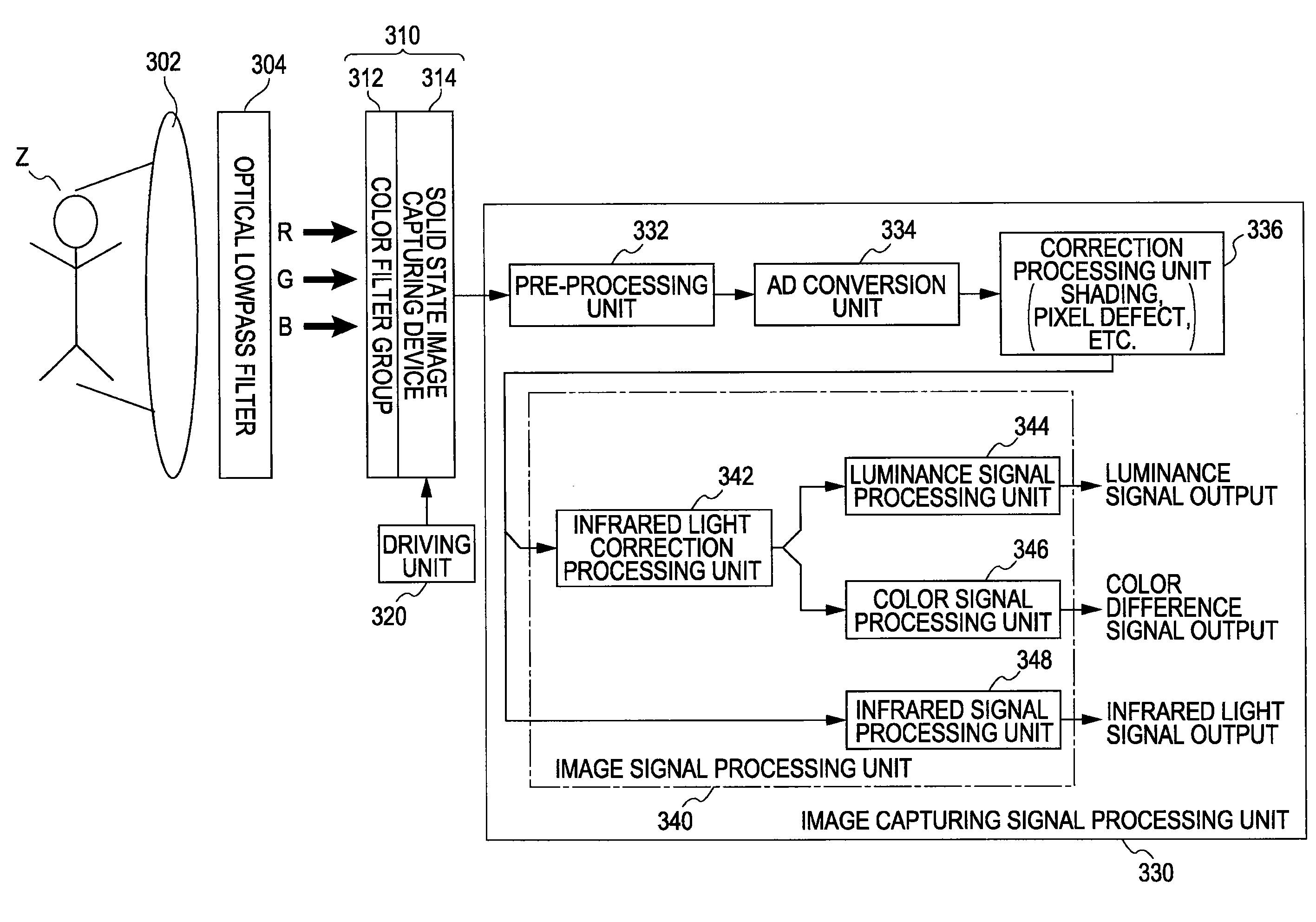
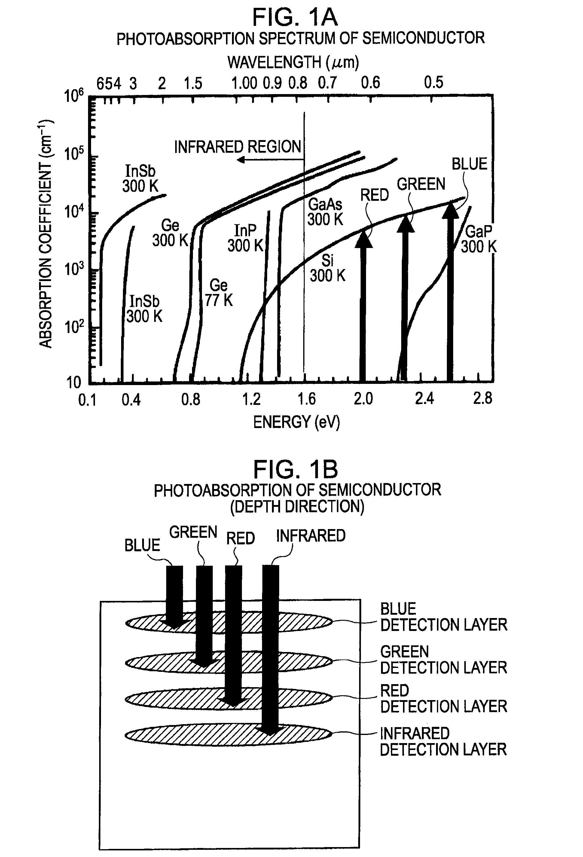
[0020] Accordingly, ways by which to receive infrared light alone, or visible light and infrared light as a signal to capture an image include removing the infrared light cut filter, or reducing the percentage for cutting infrared light.
[0027] The present invention has been made in light of the above situations. According to embodiments of the present invention, there is provided a new arrangement for eliminating influence of unnecessary wavelength region components such as infrared light, ultraviolet light, and so forth which filter in a principal wavelength region such as a visible light region.

Problems solved by technology

Accordingly, even in the event that a blue signal does not actually exist, input of a green or red signal enables a blue signal to be input, i.e., enables a false signal to be generated, and consequently, it is difficult to obtain sufficient color reproducibility.
In order to avoid this situation, signal processing can be made using calculations to perform correction as to the entire three primary colors, which calls for providing additional circuits necessary for calculations, and consequently, the circuit configuration becomes complex and great in scale, and also drives up costs.
Further, for example, upon any one of the three primary colors being saturated, it becomes difficult to recognize the original value of the saturated light, and accordingly, the calculations are incorrect, and consequently, the signal is subjected to processing to obtain color that is not the original color.

Method used


Image

  • Physical information acquisition method, physical information acquisition device, and semiconductor device
  • Physical information acquisition method, physical information acquisition device, and semiconductor device
  • Physical information acquisition method, physical information acquisition device, and semiconductor device

Examples


Embodiment Construction

[0134] Embodiments of the present invention will be described below in detail with reference to the drawings.

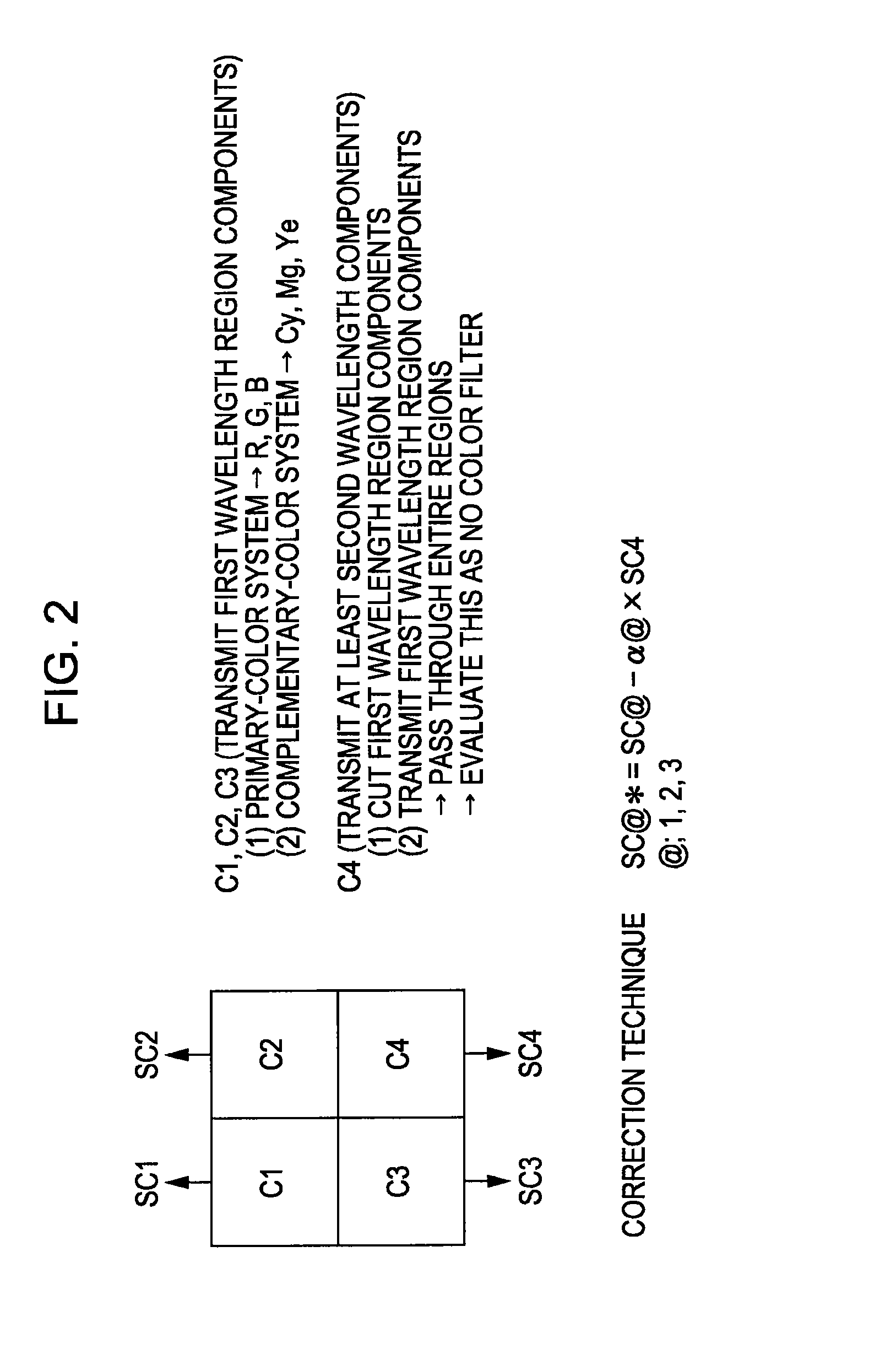
[0135]FIG. 2 is a diagram illustrating the basic configuration of a layout example of color separation filters which constantly enable a visible light color image and an infrared light image to be obtained independently using correction computing. Here, four types of color filters having distinct filter properties are disposed regularly (a tetragonal lattice in the present embodiment), which are made up of color filters C1, C2, and C3 for visible light color images (any of these transmits the first wavelength region components) serving as filters for three wavelength regions (color components), and a color filter C4 for infrared light serving as second wavelength region components different from the components of the color filters C1, C2, and C3. The respective components can be detected independently by the corresponding detection unit through the color filters C1, C2, C3, ...


PUM


Abstract

A physical information acquisition device uses a device including a detection unit for detecting electromagnetic waves, and a unit signal generating unit for generating and outputting the corresponding unit signal based on the amount of electromagnetic waves detected by the detection unit for detecting a physical quantity distribution in which the unit components are disposed on the same substrate in a predetermined sequence, for acquiring physical information for a predetermined application based on the unit signal. The physical information acquisition device includes a first detection unit which detects first wavelength region components following second wavelength region components different from the first wavelength region components being separated from the first wavelength region components beforehand; a second detection unit which detects wavelength region components for correction including at least the second wavelength region components; and a signal processing unit for obtaining physical information relating to the first wavelength region components from which at least a part of influence of the second wavelength region components is eliminated using the unit signal detected by the first detection unit, and the unit signal detected by the second detection unit.

Description

CROSS REFERENCES TO RELATED APPLICATIONS [0001] The present application claims priority to and contains subject matter related to Japanese Patent Application JP 2005-211002 filed in the Japanese Patent Office on Jul. 21, 2005 and Japanese Patent Application JP 2006-133412 filed in the Japanese Patent Office on May 12, 2006, the entire contents of which are incorporated herein by reference. BACKGROUND OF THE INVENTION [0002] 1. Field of the Invention [0003] The present invention relates to a physical information acquisition method, a physical information acquisition device, and a semiconductor device. In more detail, the present invention relates to a signal acquisition technique appropriate for applying to a solid image capturing apparatus and so forth which use a semiconductor device for physical quantity distribution detection which is configured of multiple unit components, having sensitivity as to electromagnetic waves to be input from the outside such as light, radiation, or th...

Claims


Application Information

Patent Timeline
IPC IPC(8): G06K9/00G03B11/00G01J5/00H04N9/07
CPCH04N9/735H04N9/045H01L27/14647H04N25/70H04N25/133H04N25/136H04N25/00H04N23/10H04N23/88H04N5/33H04N9/64
Inventor TODA, ATSUSHISATO, GENTA
Owner SONY CORP
Learn More