Semiconductor device

a technology of a semiconductor and a shielding circuit, which is applied in the direction of superconductor devices, semiconductor/solid-state device details, line-transmission details, etc., can solve the problem of level shifter circuits that are connected to true and bar signals that are not working properly, and achieve the effect of preventing circuits from malfunctioning

Active Publication Date: 2007-09-06
RENESAS ELECTRONICS CORP
View PDF7 Cites 10 Cited by
  • Summary
  • Abstract
  • Description
  • Claims
  • Application Information

AI Technical Summary

Benefits of technology

[0011]In view of the above circumstances, an object of the present invention is to provide a technique which reduces the influence of external noise such as crosstalk noise to prevent a circuit from malfunctioning.
[0017]Firstly, since signals susceptible to noise such as true and bar signals are shielded, the influence of external noise such as crosstalk noise is reduced, thereby preventing a circuit from malfunctioning.

Problems solved by technology

Here, if automatic routing should be done using a P&R tool as usual, true and bar signals might be affected by crosstalk noise or the like, resulting in malfunctioning of the level shifter circuit to which the true and bar signals are connected.

Method used


Image

  • Semiconductor device
  • Semiconductor device
  • Semiconductor device

Examples


first embodiment

[0034]FIGS. 3(a) to 3(c) show the arrangement of signal wires and shield wires in an I / O cell in a semiconductor device according to the first embodiment of the present invention; FIG. 4 schematically shows signal wires and shield wires with I / O cells in place; FIG. 5 schematically shows long-distance wiring with first layer metal (metal 1) shield wires; FIGS. 6(a) and 6(b) show the arrangement of signal wires and shield wires in an I / O cell and surrounding power wires; and FIG. 7 schematically shows surrounding power wires over the first layer metal (metal 1) shield wires.

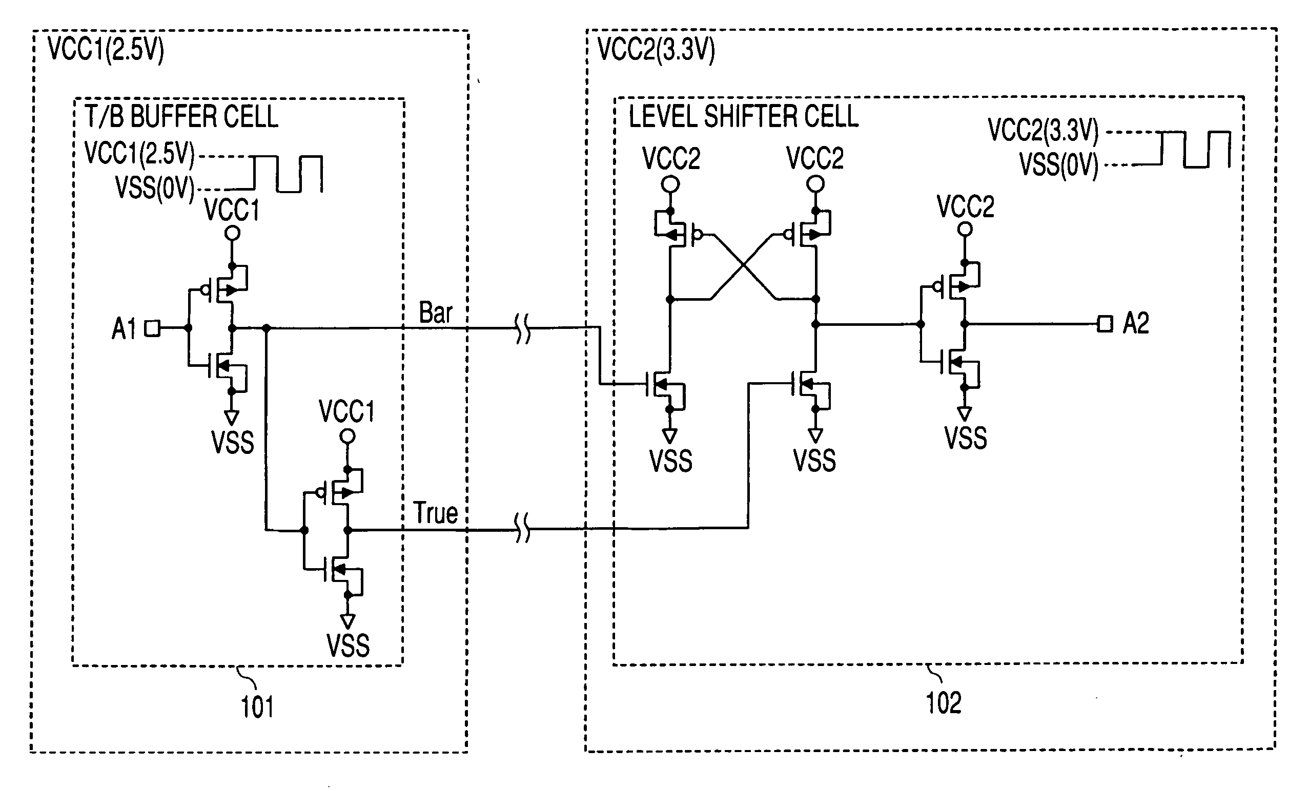
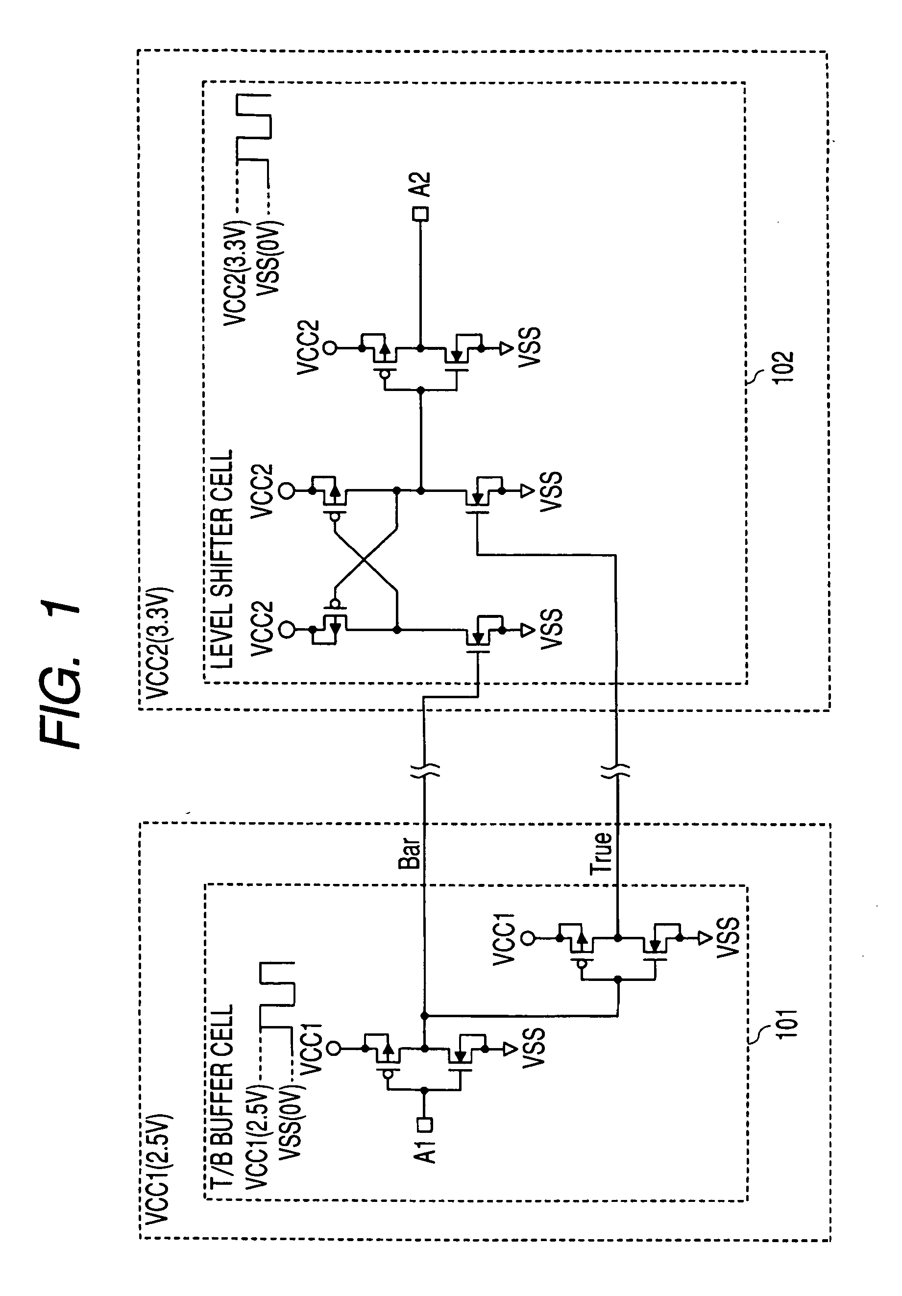
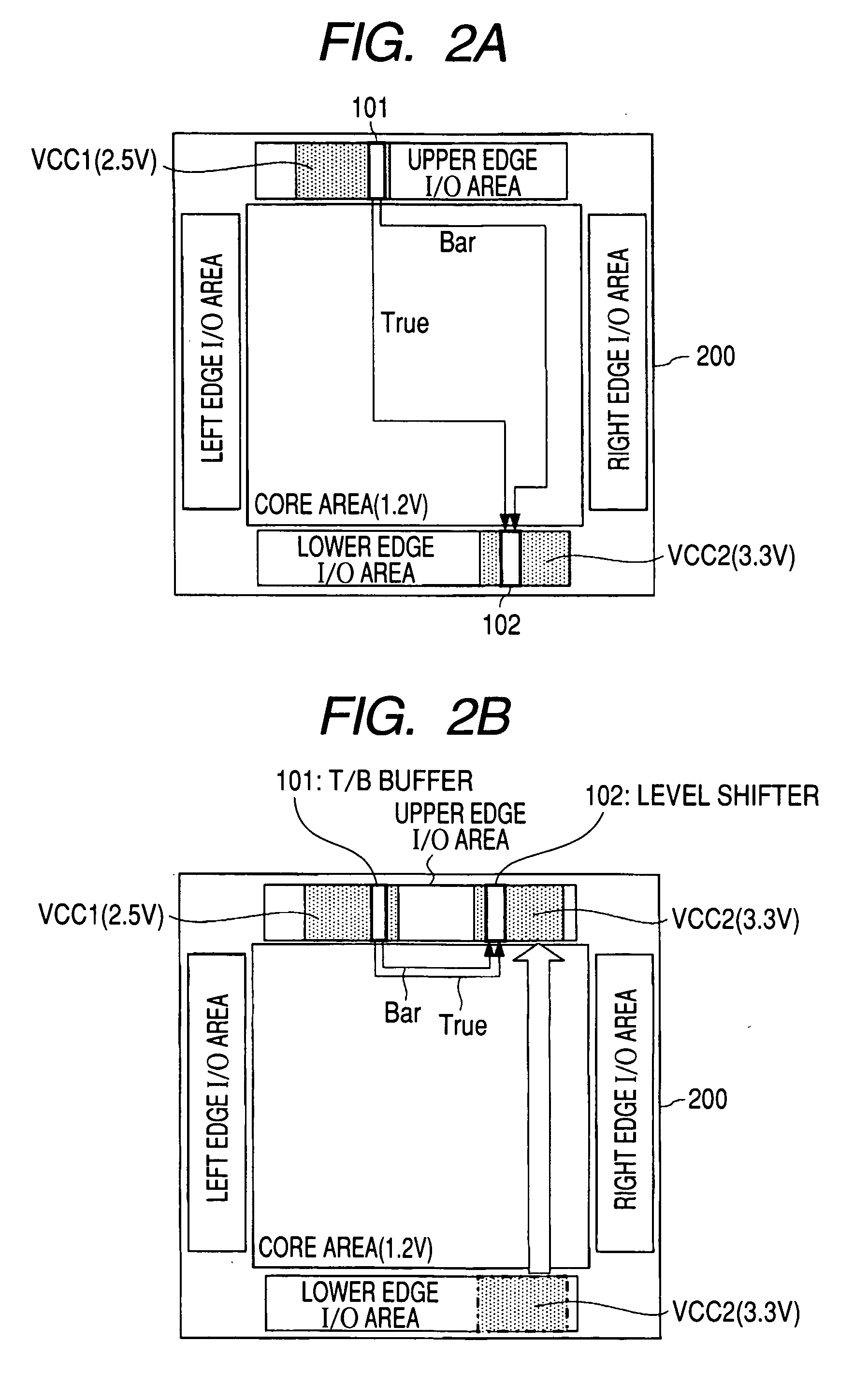
[0035]First, the arrangement of shield wires in an I / O cell 301 in the first embodiment will be explained referring to FIGS. 3(a) to 3(c). FIG. 3(a) is a top view of the I / O cell. As shown in FIG. 3(a), the I / O cell 301 has a bonding pad 302, a true signal wire 303, shield wires for it, 304a, 304b and a bar signal wire 305 and shield wires for it, 306a, 306b. The true signal and bar signal (inverted signal of the ...

second embodiment

[0050]FIGS. 8(a) to 8(c) show the arrangement of signal wires and shield wires in an I / O cell of a semiconductor device according to a second embodiment of the present invention.

[0051]While in the first embodiment a pair of two wires, a true signal wire and a bar signal wire, are formed parallel to each other in the first layer metal, the wiring structure in the second embodiment is different. In the second embodiment, the signal wires are formed in the first layer metal (metal 1) and the third layer metal (metal 3). In other words, the second embodiment employs a multilayered wiring structure in which true and bar signal wires and shield wires are vertically stacked.

[0052]The arrangement of shield wires in an I / O cell 301a in the second embodiment will be explained below referring to FIGS. 8(a) to 8(c). FIG. 8(a) is a top view of an I / O cell. As shown in FIG. 8(a), an I / O cell 301a has a bonding pad 302a, a true signal wire 303, shield wires for it, 304a, 304b, and, under these wir...


PUM


Abstract

A technique which reduces the influence of external noise such as crosstalk noise in a semiconductor device to prevent a circuit from malfunctioning. A true signal wire and a bar signal wire which are susceptible to noise and part of an input signal line to a level shifter circuit, and shield wires for shielding these signal wires are laid on an I / O cell. Such I / O cells are placed side by side to complete a true signal wire connection and a bar signal wire connection. These wires are arranged in a way to pass over a plurality of I / O cells and are parallel to each other or multilayered.

Description

CROSS-REFERENCE TO RELATED APPLICATION[0001]The present application claims priority from Japanese patent application No. 2006-57146 filed on Mar. 3, 2006, the content of which is hereby incorporated by reference into this application.BACKGROUND OF THE INVENTION[0002]The present invention relates to a semiconductor device and more particularly to a technique which is useful for the I / O cell architecture and layout method of the same.[0003]In this connection, the present inventors examined the semiconductor device technique described below.[0004]Regarding I / O (input / output circuit) areas of an LSI (large-scale integrated circuit), in transmitting signals between areas with different voltages, particularly from an I / O area with a low voltage to an I / O area with a high voltage, it is necessary to shift up the signal level.[0005]Moreover, in this case, layout of the level-up circuit requires high noise sensitivity in wiring for generating signals.[0006]In shifting up the level of a signa...

Claims


Application Information

Patent Timeline
Patent Type & Authority Applications(United States)
IPC IPC(8): H04M1/76H04M7/00H04M9/00
CPCH04B3/32
Inventor SASAKI, TAKAYUKIIGARASHI, YASUTOMORINO, NAOZUMI
Owner RENESAS ELECTRONICS CORP
Why Eureka
Try Eureka