Semiconductor device

a semiconductor device and semiconductor technology, applied in semiconductor devices, microelectromechanical systems, semiconductor/solid-state device details, etc., can solve the problems of unstable installation of semiconductor devices mounted on printed circuit boards, difficulty in precisely arranging the cover member in connection with the printed board, and difficulty for human operators (or workers)

Active Publication Date: 2007-09-13
INFINEON TECH AG
View PDF13 Cites 51 Cited by
  • Summary
  • Abstract
  • Description
  • Claims
  • Application Information

AI Technical Summary

Benefits of technology

[0013] It is an object of the present invention to provide a semiconductor device, which can be downsized without changing the size of a semiconductor sensor chip and which can be mounted on a printed-circuit board in a stable manner.

Problems solved by technology

This makes the installation of the semiconductor device mounted on the printed-circuit board unstable.
It may be possible to combine the technical features of the aforementioned semiconductor devices; however, when the semiconductor device mounted on the printed-circuit board vibrates, the diaphragm may not accurately detect pressure variations due to vibration.
In other words, fine precision is required to prevent electrical discontinuity between the conductive layer of the cover member and the connection terminals of the printed board; hence, it is troublesome for the human operator (or worker) to precisely arrange the cover member in connection with the printed board.

Method used


Image

  • Semiconductor device
  • Semiconductor device
  • Semiconductor device

Examples


first embodiment

1. First Embodiment

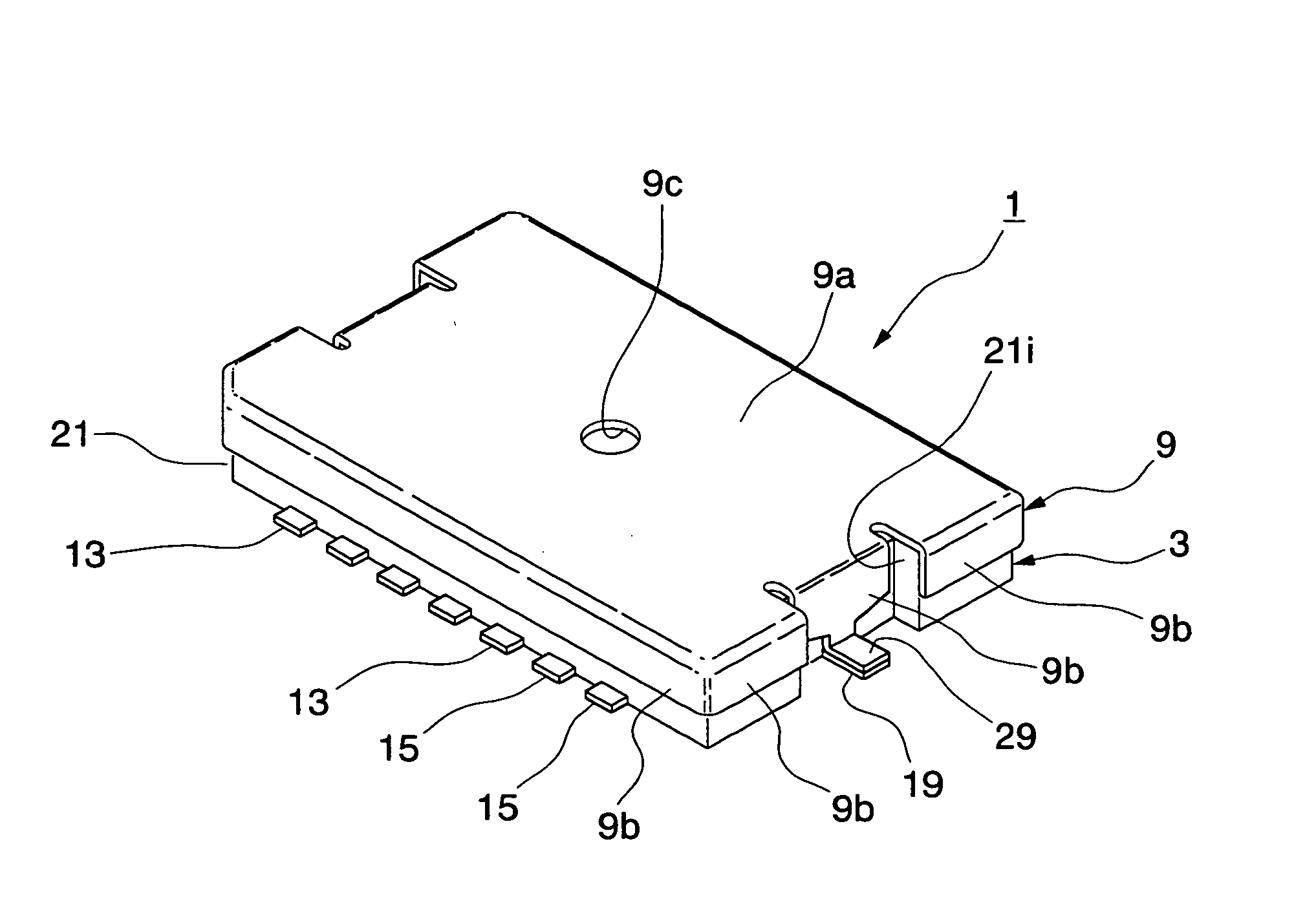
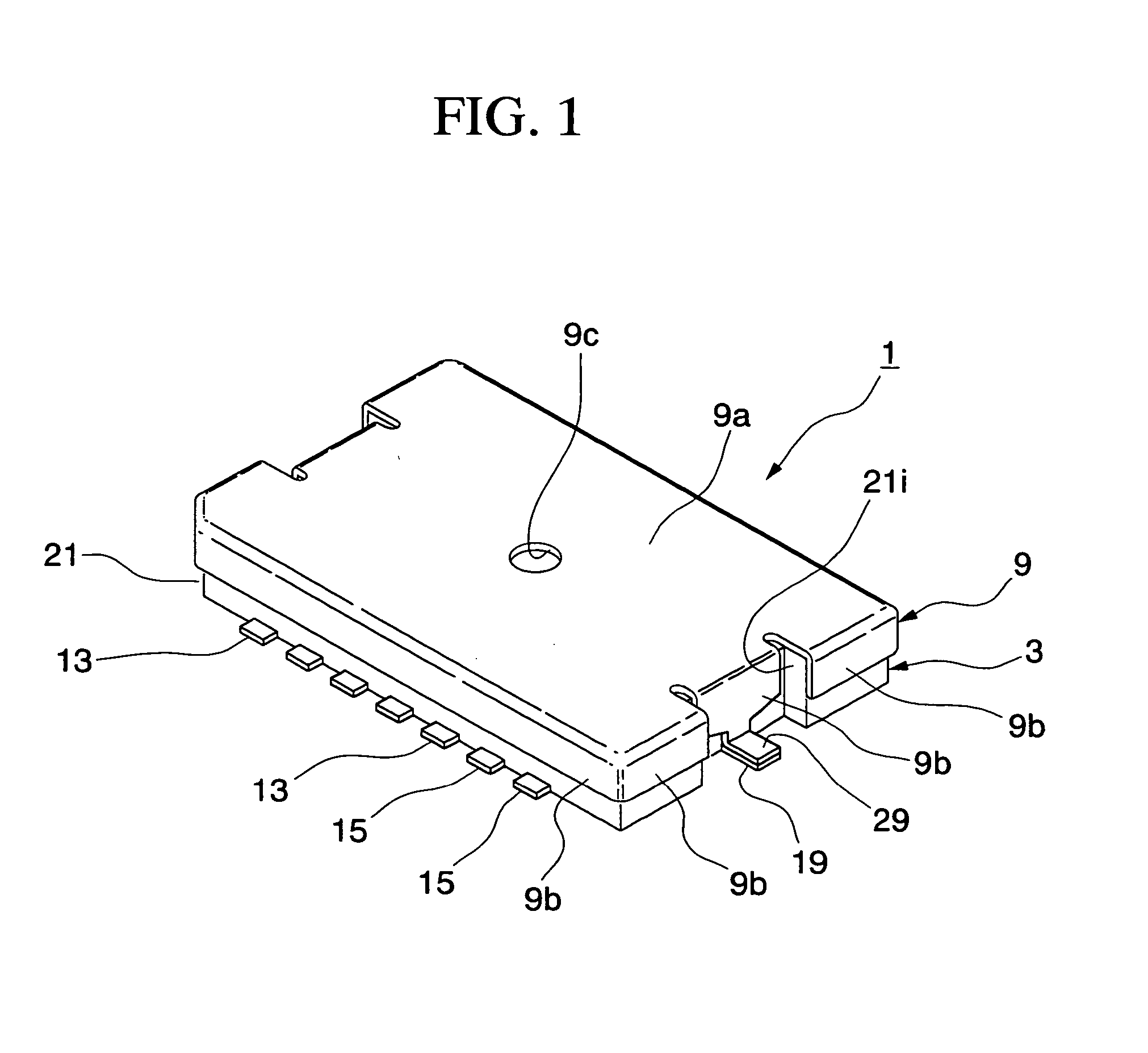
[0131] With reference to FIGS. 1 to 7, a semiconductor device 1 will be described in detail in accordance with a first embodiment of the present invention. The semiconductor device 1 of the first embodiment is designed to detect sound pressure such as sound pressure generated externally thereof and in particular directed to a surface-mount-type semiconductor device, which is manufactured using a lead frame. Specifically, the semiconductor device 1 is of the SON (i.e., Small Outline Non-leaded package) type corresponding to the surface mount type.

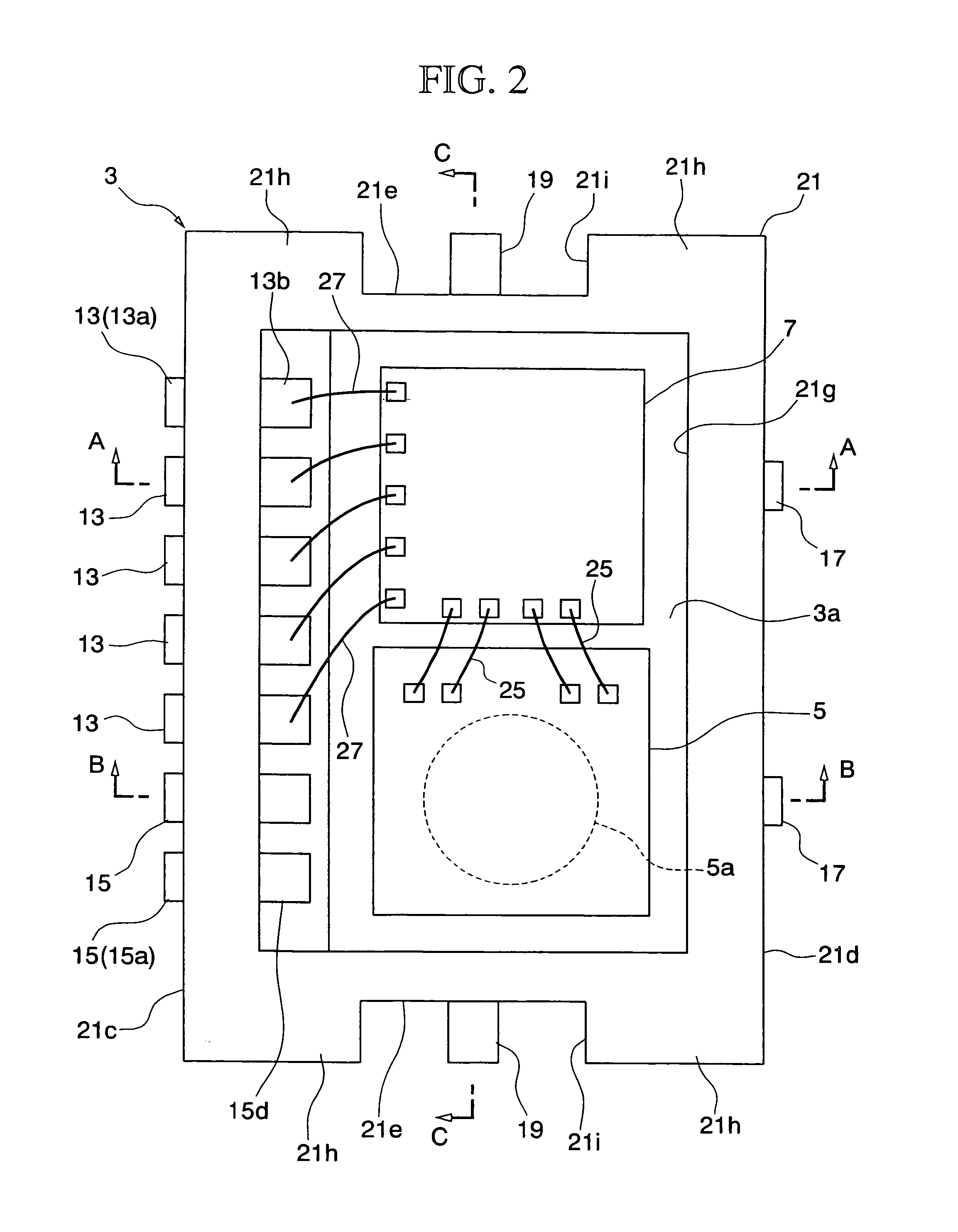
[0132] As shown in FIGS. 1, 2, and 6, the semiconductor device 1 includes a substrate 3 having a rectangular shape in plan view, and a semiconductor sensor chip 5 and an amplifier 7, both of which are arranged on an upper surface 3a of the substrate 3, and a cover member 9, which covers the semiconductor sensor chip 3 and the amplifier 7 on the substrate 3.

[0133] As shown in FIGS. 2 to 6, the substrate 3 has a stage 11 h...

second embodiment

2. Second Embodiment

[0205] A semiconductor device 100A of a second embodiment will be described in detail with reference to FIGS. 12 to 17, FIGS. 18A and 18B, and FIG. 19. The semiconductor device 100A is of a QFN (Quad Flat Non-leaded package) type and is designed to detect sound pressure.

[0206] As shown in FIGS. 12 to 16, the semiconductor device 100A includes a stage 101 having a rectangular shape; a plurality of external terminals 102 whose first ends 102a are connected to the stage 101 and whose second ends 102b extend externally of the semiconductor device 100A; a plurality of leads 103 which extend from the prescribed sides of the semiconductor device 100A toward the stage 101 so that first ends 103a thereof are positioned in proximity to the stage 101; a resin layer 104 which seals the stage 101, the external terminals 102, and the leads 103 therein and which has an opening hole 104c running through from an upper surface 104a (substantially matching the upper surface of a s...

third embodiment

3. Third Embodiment

[0274] Next, a third embodiment of the present invention will be described in detail with reference to FIGS. 28 to 30. The third embodiment is directed to a semiconductor device of an SOP (Small Outline Package) type, which is a surface mount type package manufactured using a lead frame.

[0275] As shown in FIGS. 28 to 30, a semiconductor device 201 includes a substrate 203 having a rectangular shape; a semiconductor sensor chip 205 and an amplifier 207, which are attached onto an upper surface 203a of the substrate 203; a cover member 209 for covering the upper portion of the substrate 203 including the semiconductor sensor chip 205 and the amplifier 207; and a stage 211 having a flat-plate-like shape, which is positioned below the semiconductor sensor chip 205 and the amplifier 207 and which forms the upper surface 203a of the substrate 203.

[0276] A plurality of leads 213 are formed on both sides of the stage 211, and a lead 215 is formed on the prescribed side ...


PUM


Abstract

A semiconductor device is designed such that a semiconductor sensor chip having a diaphragm for detecting pressure variations based on the displacement thereof is fixed onto the upper surface of a substrate having a rectangular shape, which is covered with a cover member so as to form a hollow space embracing the semiconductor sensor chip between the substrate and the cover member. Herein, the substrate is sealed with a molded resin such that chip connection leads packaging leads are partially exposed externally of the molded resin; the chip connection leads are electrically connected to the semiconductor sensor chip and are disposed in line along one side of the semiconductor sensor chip; and the packaging leads are positioned opposite the chip connection leads by way of the semiconductor sensor chip. Thus, it is possible to downsize the semiconductor device without substantially changing the size of the semiconductor sensor chip.

Description

BACKGROUND OF THE INVENTION [0001] 1. Field of the Invention [0002] The present invention relates to semiconductor devices including semiconductor sensor chips for detecting variations of pressure such as variations of sound pressure applied thereto. [0003] This application claims priority on seven Japanese Patent Applications whose numbers are 2005-376396, 2005-354458, 2006-48351, 2006-21164, 2005-354459, 2006-303717, and 2006-303837, the contents of which are incorporated herein by reference. [0004] 2. Description of the Related Art [0005] Conventionally, semiconductor devices such as silicon-capacitor microphones and pressure sensors, in which semiconductor chips having thin-film diaphragms for detecting variations of sound pressure are mounted on the surfaces of the printed boards, have been developed. For example, Japanese Patent Application Publication No. 2004-537182 teaches an example of a silicon-capacitor microphone. This kind of semiconductor senor chip detects variations...

Claims


Application Information

Patent Timeline
Patent Type & Authority Applications(United States)
IPC IPC(8): H01L29/82
CPCB81B7/007B81B2201/0257H01L2924/3025H01L2924/3011H01L2224/49171H01L2224/48247H01L2224/48137H01L2224/48091H01L2224/45139B81C1/0023B81B2201/0264H01L2924/00014H01L2924/00H01L2924/15153H01L2924/00011H01L2224/45015H01L2924/207H01L2924/01049H01L23/12H01L23/32
Inventor SAKAKIBARA, SHINGOSAITOH, HIROSHISUZUKI, TOSHIHISA
Owner INFINEON TECH AG
Why Eureka
Try Eureka