Organic light emitting diode display device and method for fabricating the same

Inactive Publication Date: 2007-09-13
SAMSUNG MOBILE DISPLAY CO LTD
View PDF6 Cites 16 Cited by
  • Summary
  • Abstract
  • Description
  • Claims
  • Application Information

AI Technical Summary

Benefits of technology

[0026]Accordingly, an aspect of the present invention is designed to solve such drawbacks, and therefore an object of the present invention is to provide an organic light emitting diode display capable of preventing a phenomenon of Newton's rin

Problems solved by technology

Also, the organic light emitting diode display further includes an encapsulation substrate so that the organic light emitting diode device can be isolated from the outside environment to prevent moisture from being penetrated since a life span of the display may be shortened due to oxidation, peeling, etc. of electrode materials, and therefore a luminescence efficiency may be deteriorated if moisture and oxygen flow in from the neighboring environment.
However, the mentioned-above organic light emitting diode display includes a polarizer attached to a top surface of the encapsulation substrate so as to prevent a contrast of the organic light emitting diode device from being deteriorated by reflection of an external light since the contrast may be deteri

Method used


Image

  • Organic light emitting diode display device and method for fabricating the same
  • Organic light emitting diode display device and method for fabricating the same
  • Organic light emitting diode display device and method for fabricating the same

Examples


first embodiment

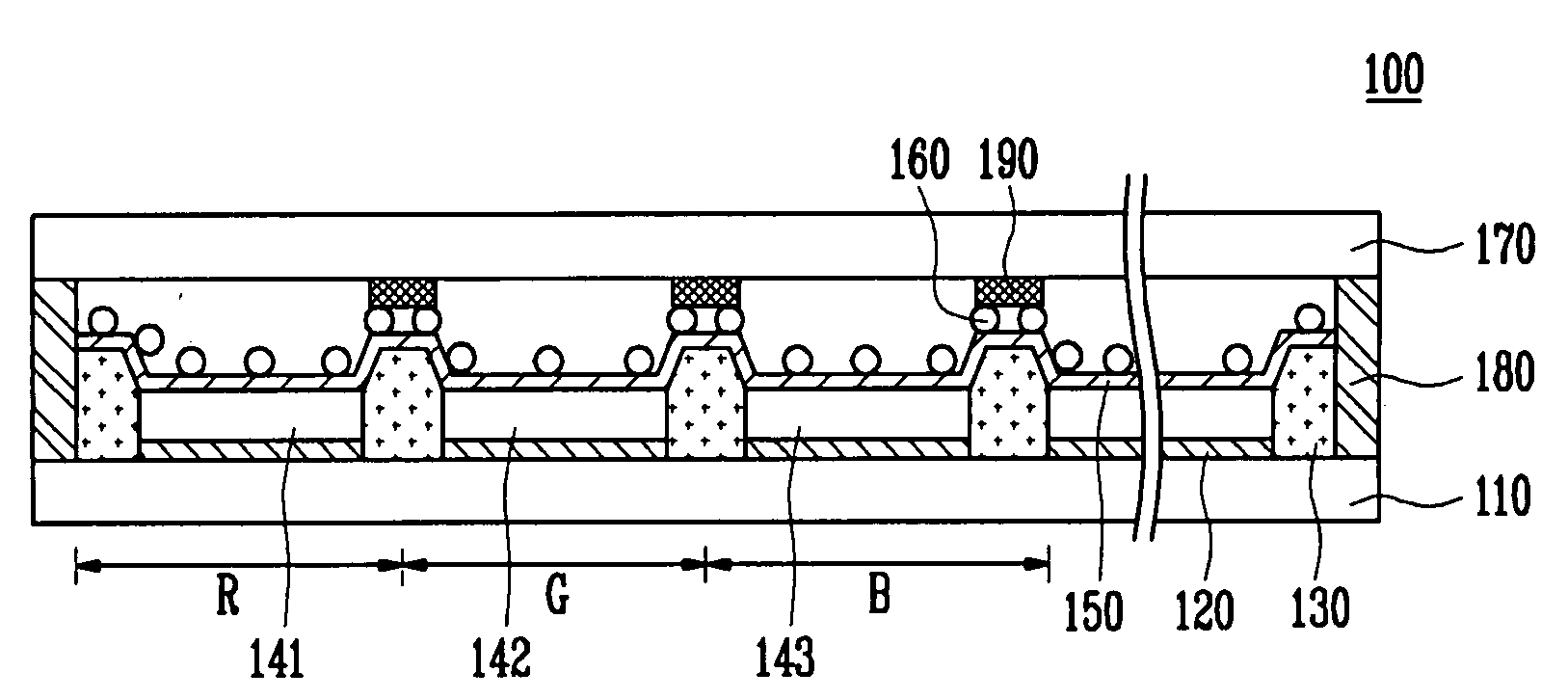
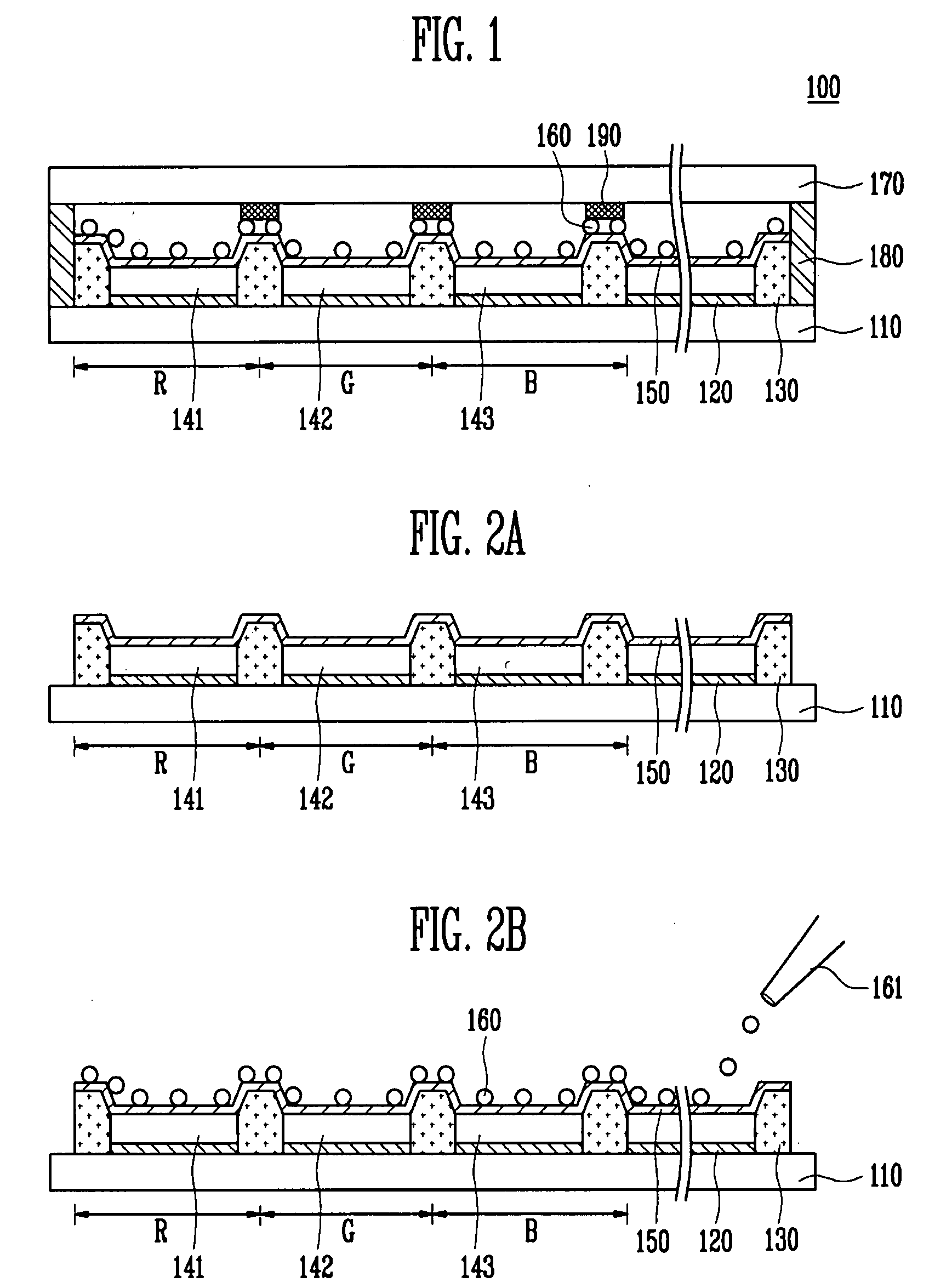
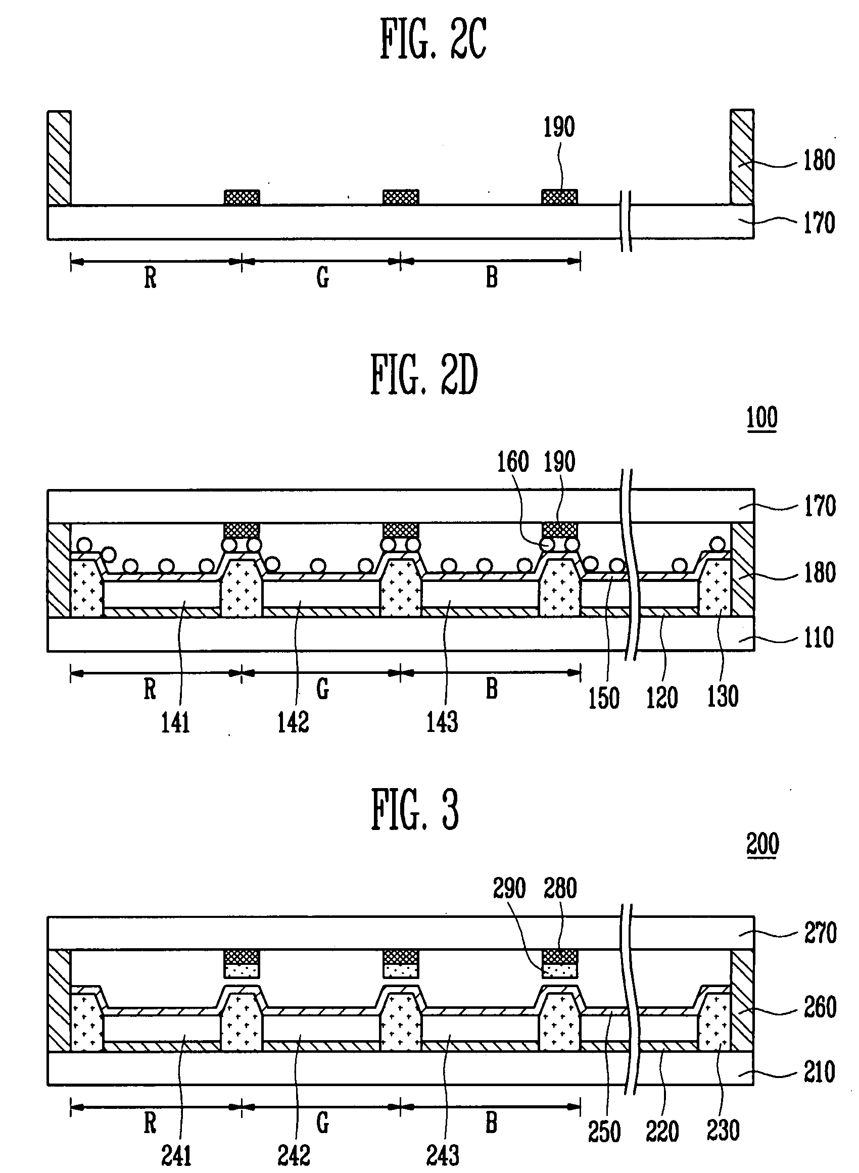
[0039]FIG. 1 is a cross-sectional view showing an organic light emitting diode display according to the present invention.

[0040]Referring to FIG. 1, the organic light emitting diode display 100 includes a first substrate 110 including at least one pixel selected from the group consisting of a plurality of red (R), green (G) and blue (B) subpixels; and a second substrate 170 arranged to be overlapped with the first substrate 110 and having black matrix 190 respectively formed in positions corresponding to the subpixels and interfaces of the subpixels, wherein the organic light emitting diode display 100 has a spacer 160 between the first substrate 110 and the second substrate 170.

[0041]On the first substrate 110 is formed a plurality of pixels selected from the group consisting of red (R), green (G) and blue (B) subpixels. Each of the subpixels (R,G,B) includes a thin film transistor and an organic light emitting diode device. The organic light emitting diode device includes a first ...

second embodiment

[0056]FIG. 3 is a cross-sectional view showing an organic light emitting diode display according to the present invention.

[0057]In order to avoid an overlapped description, detailed descriptions of the same components as in the mentioned-above first embodiment, for example a first substrate 110, a first electrode 120, a second electrode 170 and a black matrix 190 are omitted.

[0058]Referring to FIG. 3, the organic light emitting diode display 200 includes a first substrate 210 including at least one pixel selected from the group consisting of a plurality of red (R), green (G) and blue (B) subpixels; and a second substrate 270 arranged to be overlapped with the first substrate 210 and having black matrix 280 respectively formed in positions corresponding to the subpixels and interfaces of the subpixels, wherein a spacer 290 is formed on the black matrix 280.

[0059]The first electrode 220 is patterned on the first substrate 210 having subpixel regions of the red (R), green (G) and blue ...

third embodiment

[0069]FIG. 5 is a cross-sectional view showing an organic light emitting diode display according to the present invention.

[0070]In order to avoid an overlapped description, detailed descriptions of the same components as in the mentioned-above first embodiment, for example a first substrate 110, a first electrode 120, a second electrode 170 and a black matrix 190 are omitted.

[0071]Referring to FIG. 5, the organic light emitting diode display 300 includes a first substrate 310 including at least one pixel selected from the group consisting of a plurality of red (R), green (G) and blue (B) subpixels; a spacer 380 arranged to be overlapped with the first substrate 310 and respectively formed with a predetermined pattern in positions corresponding to the subpixels and interfaces of the subpixels on a lower surface of the second substrate 370; and a black matrix 390 formed on the spacer 380.

[0072]On the first substrate 310 are formed a plurality of pixels selected from the group consisti...


PUM


Abstract

Disclosed is an organic light emitting diode display capable of preventing a phenomenon of Newton's rings by maintaining a constant gap between a first substrate and a second substrate, and a method for fabricating the same. The organic light emitting diode display includes a first substrate including at least of pixel selected from the group consisting of a plurality of red, blue and green subpixels; and a second substrate arranged to be overlapped with the first substrate and having black matrixes respectively formed in positions corresponding to the subpixels and interfaces of the subpixels, wherein the organic light emitting diode display has a spacer between the first substrate and the second substrate.

Description

CROSS-REFERENCE TO RELATED APPLICATIONS[0001]This application claims the benefit of Korean Patent Application No. 2006-0021889, filed on Mar. 8, 2006 and 2006-0067393, filed on Jul. 19, 2006, in the Korean Intellectual Property Office, the disclosure of which is incorporated herein by reference.BACKGROUND[0002]1. Field of the Invention[0003]The present invention relates to an organic light emitting diode display and a method for fabricating the same, more specifically to an organic light emitting diode display capable of preventing a phenomenon of Newton's rings by further forming a spacer between a first substrate and a second substrate having a black matrix formed therein, thereby to maintain a constant gap between the first substrate and the second substrate, and a method for fabricating the same.[0004]2. Discussion of Related Art[0005]In recent years, the organic light emitting diode display has been widely used in this field and has a relatively simple configuration. The organi...

Claims


Application Information

Patent Timeline
IPC IPC(8): H05B33/00H01L51/50
CPCH01L27/3295H01L51/56H01L51/5237H10K59/122H10K50/8428H10K71/00
Inventor SONG, SEUNG YONGLEE, KWAN HEE
Owner SAMSUNG MOBILE DISPLAY CO LTD
Why Eureka
Try Eureka