Semiconductor device, ink cartridge, and electronic device

a technology of ink cartridges and semiconductors, applied in the direction of testing/measurement of semiconductor/solid-state devices, printing, electrical equipment, etc., can solve the problems of complex sensor structure, waste of remaining ink, and errors in the amount of ink consumed, and achieve high reliability and high-quality

Inactive Publication Date: 2007-09-13
SEIKO EPSON CORP
View PDF0 Cites 8 Cited by
  • Summary
  • Abstract
  • Description
  • Claims
  • Application Information

AI Technical Summary

Benefits of technology

[0077]Obviously, a highly reliable, high-quality product can thereby be provided.

Problems solved by technology

However, this management method of using software to calculate ink consumption has problems such as the following.
Although this weight variation of the ink droplets does not affect the image quality, it causes ink consumption amount errors which accumulate in the ink cartridge.
Users have noticed that exchanging a used ink cartridge with a new one even when ink remains results in a waste of the remaining ink.
However, in Japanese Unexamined Patent Application, First Publication No. 2002-283586, the sensor structure is complex and the accompanying system also becomes complex, increasing manufacturing costs.
However, in addition to the electrical connection between the electrode terminal of the piezoelectric device and the contact terminal in the holder, at least two or more electrical contact points are required between the ink cartridge and the main device, leading to concern over the reliability of the electrical connection.
Consequently it is difficult to synthesize both types of information, and to perform simple and detailed information management such as ensuring that the ink cartridge cannot function unless it is set in the main device.
The user often becomes particularly concerned when the remaining amount of ink in the ink cartridge decreases to a small amount.

Method used


Image

  • Semiconductor device, ink cartridge, and electronic device
  • Semiconductor device, ink cartridge, and electronic device
  • Semiconductor device, ink cartridge, and electronic device

Examples


first embodiment

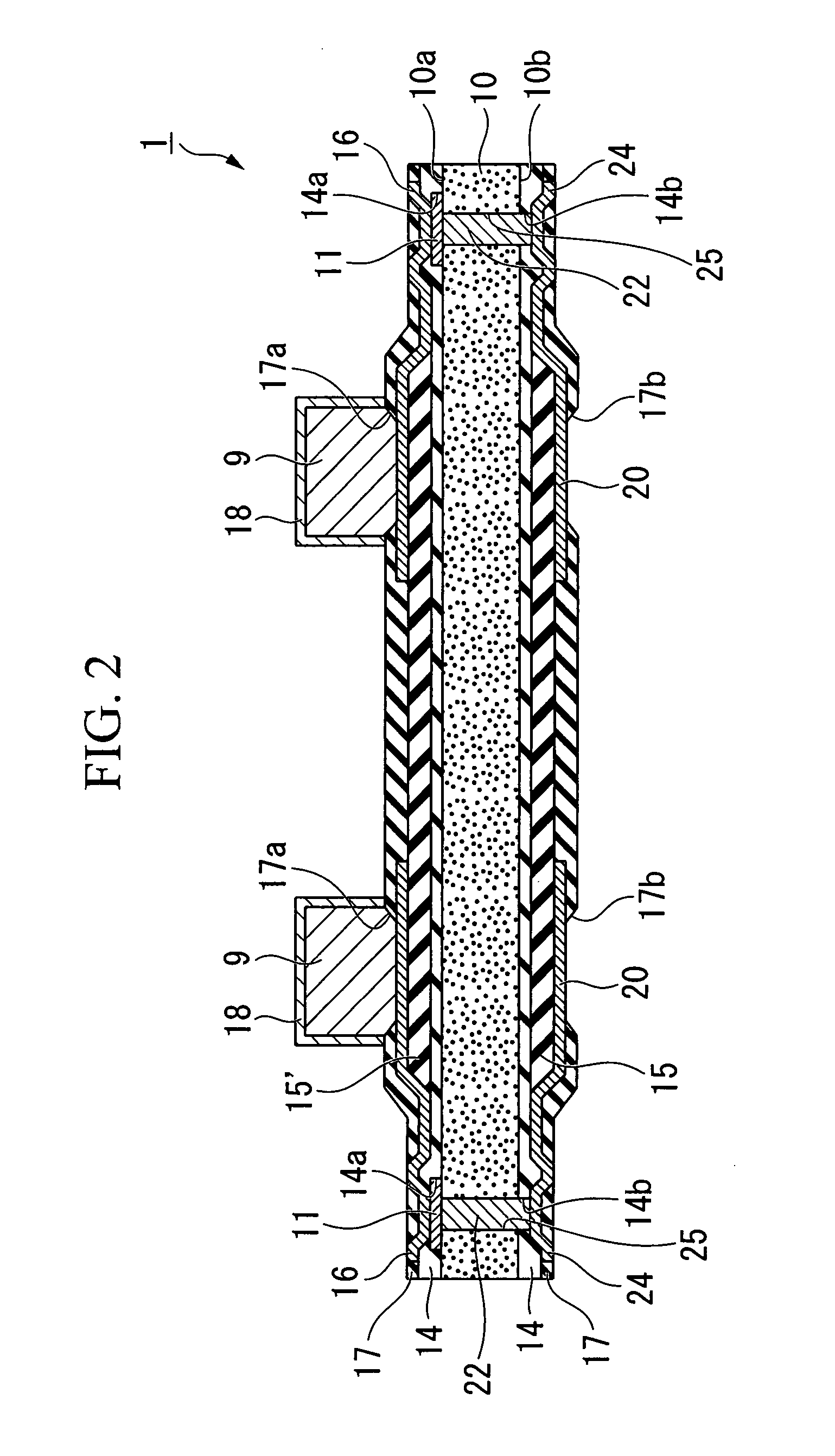
[0091]FIG. 2 is a cross-sectional view of a semiconductor device of the invention.

[0092]FIG. 3 is an exterior view of a first embodiment of a semiconductor device of the invention.

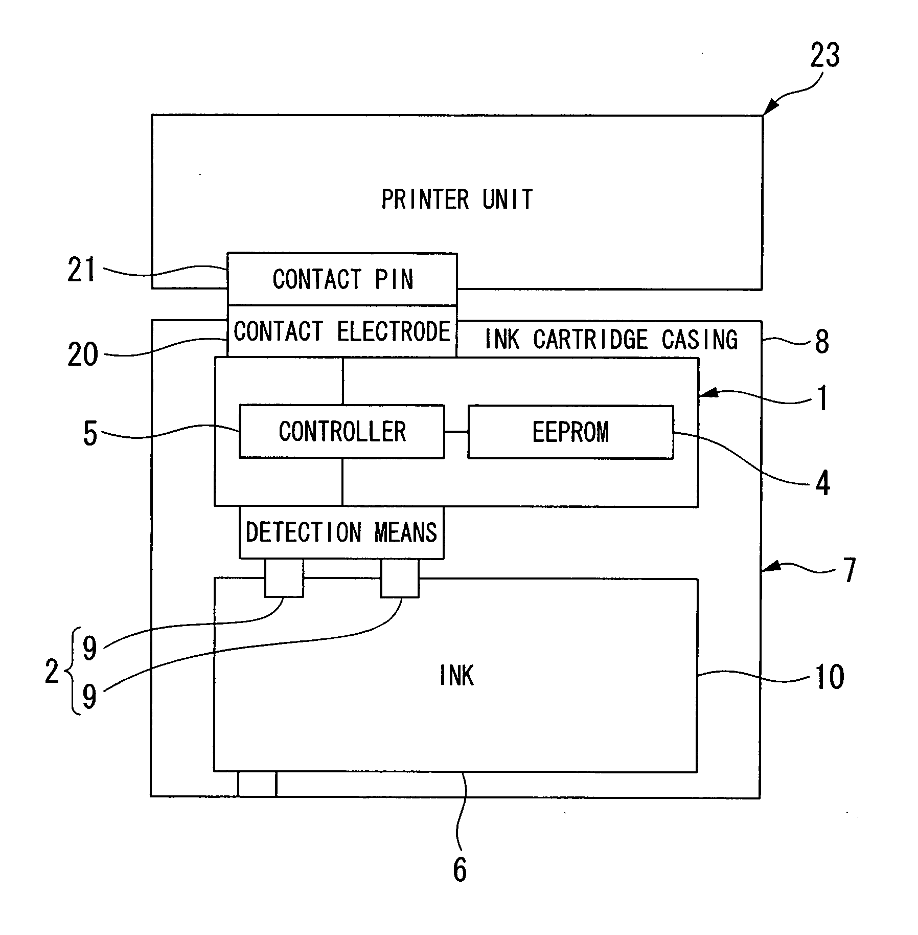
[0093]In these diagrams, reference numeral 1 represents a semiconductor device having a wafer level chip scale package (W-CSP) structure.

[0094]The semiconductor device 1 includes liquid contact electrodes 9 (detection electrodes), a connection electrodes 20 (contact electrodes), an EEPROM 4 (storage circuit), and a controller 5 (control circuit), which are provided on a rectangular semiconductor substrate 10.

[0095]The liquid contact electrodes 9 detect a remaining amount of ink.

[0096]The connection electrodes 20 transmit and receive information to or from the contact pin groups 21 of the printer unit 23.

[0097]The EEPROM 4 stores ink information.

[0098]The controller 5 collectively controls the liquid contact electrodes 9, the connection electrodes 20, and the EEPROM 4.

[0099]The semiconductor substrate 10 is...

second embodiment

[0187]Subsequently, a second embodiment will be described with reference to FIG. 5.

[0188]In FIG. 5, parts corresponding to those in FIGS. 1 to 3 are represented by like reference numerals, and are not repetitiously explained.

[0189]Reference numeral 41 represents a semiconductor device of the invention.

[0190]This embodiment differs from the first embodiment in that parts of the relocation interconnections 16 exposed via the openings 17a in the protective layer 17 over the active element formation face 10a are used as liquid contact electrodes 12 (detection electrodes).

[0191]In this embodiment, ink information is detected when the exposed parts of the relocation interconnections 16 are wetted by ink infiltrating into the openings 17a.

[0192]To achieve this, a plated layer of metal having excellent chemical resistance is formed over the relocation interconnections 16 exposed through the openings 17a in the same manner as described above.

[0193]In this embodiment, a Ni-p+Au plated film (...


PUM


Abstract

A semiconductor device includes: a semiconductor substrate including an active element formation face on which an active element is formed, and a rear face that is on a side opposite to the active element formation face; detection electrodes formed on or above the active element formation face, detecting a remaining amount of ink by being wet in the ink; a penetration electrode penetrating a thickness direction of the semiconductor substrate; and a contact electrodes formed on or above the rear face, electrically connected to the detection electrodes via the penetration electrode, and transmitting and receiving information.

Description

CROSS-REFERENCE TO RELATED APPLICATION[0001]This application claims priority on Japanese Patent Application No. 2006-067425, filed Mar. 13, 2006, the contents of which are incorporated herein by reference.BACKGROUND[0002]1. Technical Field[0003]The present invention relates to a semiconductor device, an ink cartridge, and an electronic device.[0004]2. Related Art[0005]There are conventional methods of managing ink consumption of ink cartridges in printers or the like that use ink for recording.[0006]An example of such management methods is one which calculates ink consumption by using software to integrate the number of ink droplets ejected at the recording head and the amount of ink absorbed by maintenance.[0007]However, this management method of using software to calculate ink consumption has problems such as the following.[0008]There is weight variation in the ink droplets ejected in the head.[0009]Although this weight variation of the ink droplets does not affect the image quali...

Claims


Application Information

Patent Timeline
Patent Type & Authority Applications(United States)
IPC IPC(8): B41J2/195B41J29/393B41J2/175
CPCB41J2002/17579B41J2/17566B41J2/01H01L22/00H05K3/12
Inventor HASHIMOTO, NOBUAKI
Owner SEIKO EPSON CORP
Why Eureka
Try Eureka