Approaching programmable self-assembly: heterogeneous integration of chip-scale components on planar and non-planar surfaces

a programmable self-assembly and component technology, applied in the direction of chemistry apparatus and processes, sustainable manufacturing/processing, final product manufacturing, etc., can solve the problems of difficult to adapt the self-assembly to microelectronic systems, which consists of more than one repeating unit, and the integration of components with distinct angular orientation, etc., to achieve the effect of fast delivery of components

Active Publication Date: 2007-09-20
MINNESOTA RGT UNIV OF A CORP OF MN
View PDF16 Cites 34 Cited by
  • Summary
  • Abstract
  • Description
  • Claims
  • Application Information

AI Technical Summary

Benefits of technology

[0007] Another aspect of the invention relates to an extension that combines the described self-assembly method with existing transfer solution. Chiplet transfer processes have been investigated in recent years as a means to transfer semiconducting materials and chiplets from one substrate to another. The combined solution of programmed self-assembly with transfer technology provides a unique solution to the massively parallel flip chip integration of components with minimal restrictions on the distance, location, size, and pitch of interconnects between the components and the final substrate. The self-assembly enables the massively parallel redistribution and reordering of components.

Problems solved by technology

However, the adaptation of self-assembly to microelectronic systems, which consists of more than one repeating unit, is difficult to achieve due to insufficient power of recognition.
As a result the assembly of electrically functional heterogeneous systems that are built using non-identical components has not been possible.
Another challenge is the integration of components with distinct angular orientation.
Angular orientation control has been challenging in self-assembly.
While specific designs in the shape of the receptors and binding sites have been tested to favor one orientation over the other, the removal of defects due to local energy minima and partial overlap between receptors and binding sites remain unsolved.

Method used


Image

  • Approaching programmable self-assembly: heterogeneous integration of chip-scale components on planar and non-planar surfaces
  • Approaching programmable self-assembly: heterogeneous integration of chip-scale components on planar and non-planar surfaces
  • Approaching programmable self-assembly: heterogeneous integration of chip-scale components on planar and non-planar surfaces

Examples


Embodiment Construction

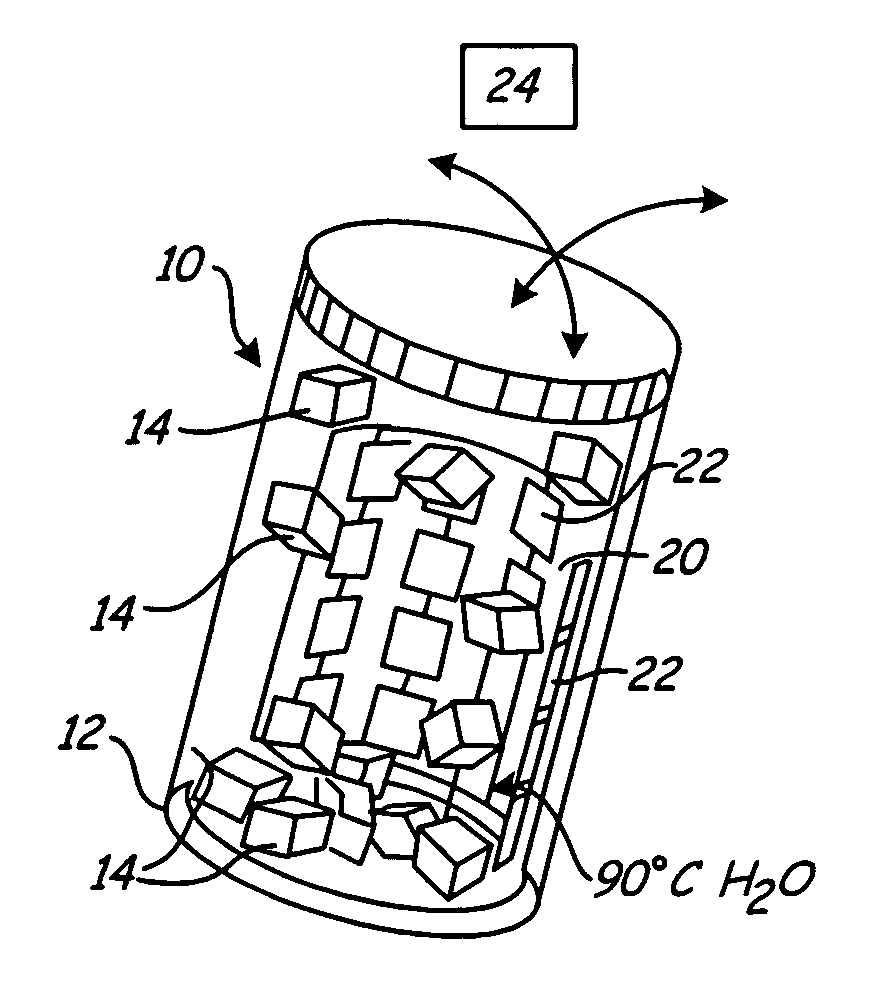
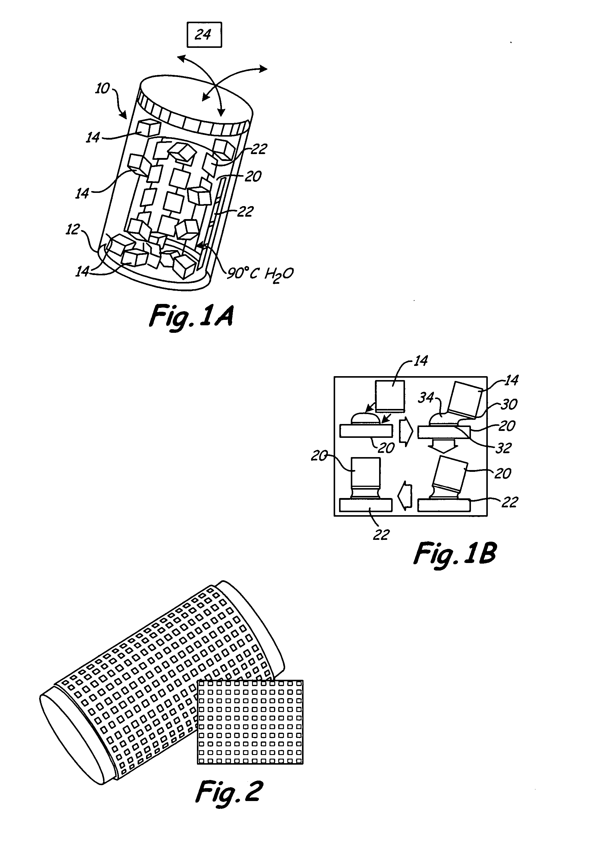
[0027] One aspect of the present invention relates to programmable reconfigurable liquid solder directed self-assembly (PRS) process to enable heterogeneous integration of components (e.g., dies, chips, chiplets) on non-planar substrates. The process makes use of solder-based receptors that can be activated locally. Metal contacts on segmented semiconductor devices bind to liquid-solder-based-receptors on a substrate surface during the fluidic self-assembly. Programmability is implemented using solder-based receptors that can be switched “ON” and “OFF” using integrated heaters or scanning lasers. The feasibility of the PRS concept has been evaluated through computer simulations using ANSYS to estimate: (i) the necessary power to heat selected receptors to above the melting point of the solder, (ii) the minimal spacing between receptors for preventing thermal crosstalk, and (iii) the effect of the liquid flow in the agitated assembly solution. We fabricated a prototype substrate to e...


PUM

PropertyMeasurementUnit
sizeaaaaaaaaaa
melting pointaaaaaaaaaa
temperatureaaaaaaaaaa

Abstract

A method of self-assembly of components on a surface of a substrate includes obtaining a first component and a second component. The first component type is assembled onto the substrate by programming the surface. The second component type is assembled by reprogramming the surface. A third component, next to the first and second components, is assembled following the step of assembling the first and second components. The first, second, and third components are all different types of components. docking sites on the substrate can be used that contain alignment pedestals. One component delivery system employ a liquid-liquid interface to deliver and concentrate components with correct pre-orientation.

Description

CROSS-REFERENCE TO RELATED APPLICATION [0001] The present application is based on and claims the benefit of U.S. provisional patent application Ser. No. 60 / 782,248, filed Mar. 14, 2006, the content of which is hereby incorporated by reference in its entirety.GOVERNMENT RIGHTS [0002] The United States government has certain rights in this invention pursuant to Agency Grant No. ECS-0300263 awarded by the National Science Foundation.BACKGROUND OF THE INVENTION [0003] Fabrication strategies that rely on mechanisms of self-assembly are widely recognized as inevitable tools in nanotechnology. Self-assembly is not limited to the nanometer length scale. Strategies that are based on self-assembly are projected to have a major impact in the manufacturing of systems on both, the micro, and nanometer length scale. Previous demonstrations of a directed self-assembly to generate functional electrical Microsystems include the coplanar integration of segmented integrated circuits (IC) using capilla...

Claims


Application Information

Patent Timeline
Patent Type & Authority Applications(United States)
IPC IPC(8): B32B37/00
CPCH01L24/31Y10T29/4913H01L24/95H01L25/50H01L2224/83192H01L2224/83801H01L2224/95085H01L2224/95146H01L2924/01005H01L2924/01029H01L2924/01074H01L2924/01079H01L2924/10329H01L2924/14H05K1/0212H05K3/303H05K3/341H05K3/3494H05K2201/10522H05K2203/048H05K2203/0776H05K2203/107H05K2203/1476H01L24/29H01L2924/01006H01L2924/01023H01L2924/01033H01L2924/014H01L2924/0132H01L24/83Y10T29/49117Y10T29/49131Y10T156/1089H01L2924/10253H01L2924/01031H01L2924/00H01L2224/8314H01L2224/26165H01L2224/29144Y02P70/50H01L2224/95136H01L2924/013H01L2924/0105H01L2924/00012
Inventor JACOBS, HEIKO O.
Owner MINNESOTA RGT UNIV OF A CORP OF MN
Why Eureka
Try Eureka