Trench capacitor structure and process for applying a covering layer and a mask for trench etching processes in semiconductor substrates

a technology of trench etching and trench capacitor, which is applied in the direction of semiconductor devices, electrical equipment, transistors, etc., can solve the problems of mask and stress relief layer having to be removed

Inactive Publication Date: 2005-06-02
POLARIS INNOVATIONS
View PDF9 Cites 3 Cited by
  • Summary
  • Abstract
  • Description
  • Claims
  • Application Information

AI Technical Summary

Benefits of technology

[0013] An object of the present invention is to provide a process for applying a relatively thick silicon nitride layer to a semiconductor substrate in which a processing operation acting on a patterned covering layer is subject to the minimum possible restrictions.

Problems solved by technology

Another drawback of masks with a silicon nitride layer and a stress relief layer of silicon dioxide beneath them is that the mask and the stress relief layer have to be removed in two steps involving a change in the etching process.

Method used


Image

  • Trench capacitor structure and process for applying a covering layer and a mask for trench etching processes in semiconductor substrates
  • Trench capacitor structure and process for applying a covering layer and a mask for trench etching processes in semiconductor substrates
  • Trench capacitor structure and process for applying a covering layer and a mask for trench etching processes in semiconductor substrates

Examples


Embodiment Construction

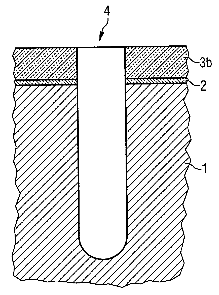
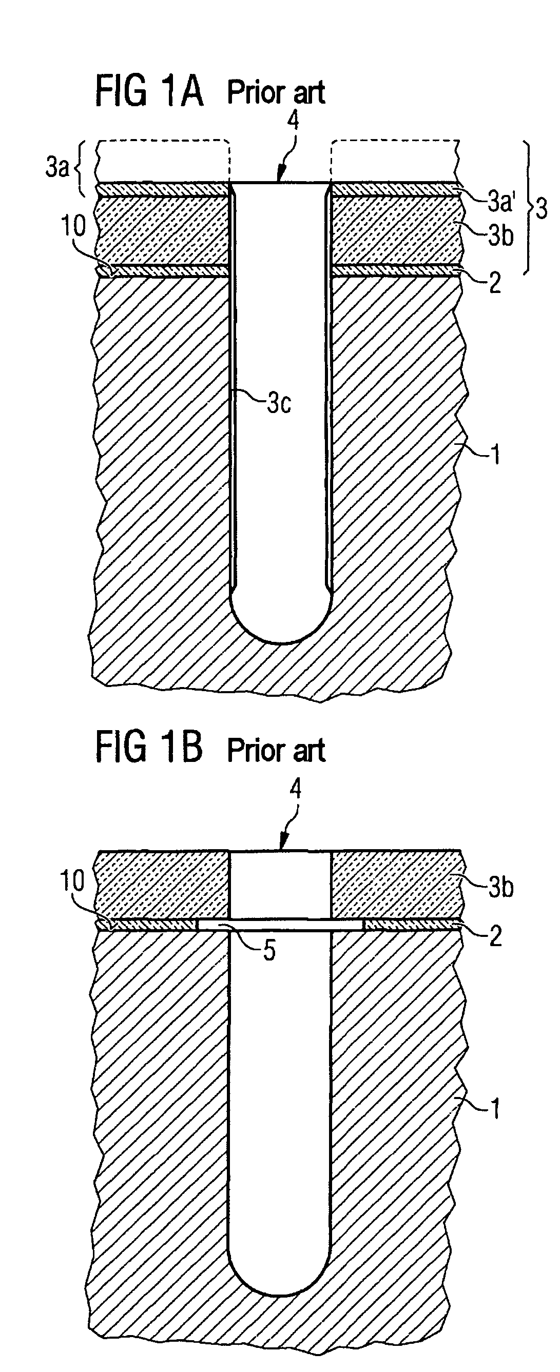
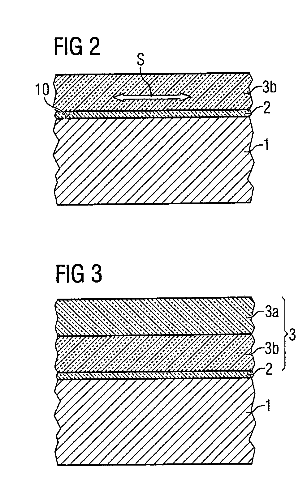
[0028] In accordance with one aspect of the present invention, a covering layer is applied to a semiconductor substrate. For this purpose, a semiconductor substrate formed from a semiconductor material is provided. A stress relief layer is provided on a process surface of the semiconductor substrate. The covering layer, which is formed from a covering material, is applied to the stress relief layer. The covering material has an expansion coefficient which differs significantly from the expansion coefficient of the semiconductor material.

[0029] According to another aspect of the invention, the stress relief layer is produced by thermal nitriding of the semiconductor material of the semiconductor substrate beneath it. According to the invention, therefore, the silicon dioxide which is customarily present as a material for stress relief layers between a semiconductor substrate and a covering layer above it with significantly different coefficients of thermal expansion is replaced by a...


PUM

PropertyMeasurementUnit
temperatureaaaaaaaaaa
thicknessaaaaaaaaaa
thicknessaaaaaaaaaa

Abstract

A stress relief layer between a single-crystal semiconductor substrate and a deposited silicon nitride layer or pad nitride is formed from thermally produced silicon nitride. The stress relief layer made from thermally produced silicon nitride replaces a silicon dioxide layer or pad oxide which is customary at this location for example in connection with mask layers. After patterning of a mask, which includes a protective layer portion formed from deposited silicon nitride, the material which is provided according to the invention for the stress relief layer reduces the restrictions imposed for subsequent process steps, such as for example wet-etching steps, acting both on the semiconductor substrate or structures in the semiconductor substrate and also on the stress relief layer. The thermal nitriding is advantageously incorporated into a preanneal step for expelling oxygen from the semiconductor substrate, so that the semiconductor substrate is protected from the etching action of the expelled oxygen by the stress relief layer which is formed, there is no need for an additional temporary etching protection layer for the semiconductor substrate and the overall processing is streamlined.

Description

CROSS REFERENCE TO RELATED APPLICATIONS [0001] This application claims priority under 35 USC §119 to German Application No. DE 103 51 031.1, filed on Oct. 31, 2003, and to German Application No. DE 10 2004 024 105.8, filed on May 14, 2004. The entire contents of these two patent applications are hereby incorporated by reference. FIELD OF THE INVENTION [0002] The invention relates to a process for applying a covering layer to a semiconductor substrate, in which the semiconductor substrate, which is formed from a semiconductor material, is provided, a stress relief layer is provided on a process surface of the semiconductor substrate, and the covering layer made from a material with an expansion coefficient that differs significantly from an expansion coefficient of the semiconductor material is applied to the stress relief layer. The invention also relates to a process for applying a mask for trench etching processes in semiconductor substrates and to a process for introducing trench...

Claims


Application Information

Patent Timeline
Patent Type & Authority Applications(United States)
IPC IPC(8): H01L21/20H01L21/308H01L21/31H01L21/314H01L21/318H01L21/334H01L21/469H01L21/8242H01L27/108H01L29/76H01L29/94H01L31/119
CPCH01L21/3081H01L21/3144H01L29/66181H01L27/1087H01L21/3185H10B12/0387H01L21/022H01L21/0217H10B12/038
Inventor BERNHARDT, HENRYSTADTMULLER, MICHAELSTORBECK, OLAFKAINZ, STEFAN
Owner POLARIS INNOVATIONS
Why Eureka
Try Eureka