Detection device and image forming device

a detection device and image technology, applied in the direction of optical radiation measurement, photometry using electric radiation detectors, instruments, etc., can solve the problems of limited detection area, difficulty in improving the photoreceptive sensitivity, and the magnitude of the device area of the photodiodes is limited to be equal or less than the wavelength, so as to improve the photoreceptive sensitivity. , the effect of improving the detection area

Inactive Publication Date: 2007-09-20
CANON KK
View PDF2 Cites 52 Cited by
  • Summary
  • Abstract
  • Description
  • Claims
  • Application Information

AI Technical Summary

Benefits of technology

[0009]Therefore, the present invention provides a detection device which solves the above-mentioned problems, has an effect of improving the photoreceptive sensitivity with respect to a generally wide frequency region including the infrared region, and has a larger detection area than that of the detection portion of the device disclosed in Tsutomu Ishii et al.; Jpn. Jour. Appl. Phys., Vol. 44 (2005), L364.

Problems solved by technology

However, in the conventional examples of the pyroelectric device using a wavelength selection filter, it is difficult to improve the photoreceptive sensitivity.
Further, in the conventional example in which photodiodes are integrated in the center of the metal diffraction ring, even though the effect of improving the photoreceptive sensitivity is provided, the magnitude of device area of the photodiodes is limited to be equal to or less than the wavelength, so that the detection area is limited.

Method used


Image

  • Detection device and image forming device
  • Detection device and image forming device
  • Detection device and image forming device

Examples


example 1

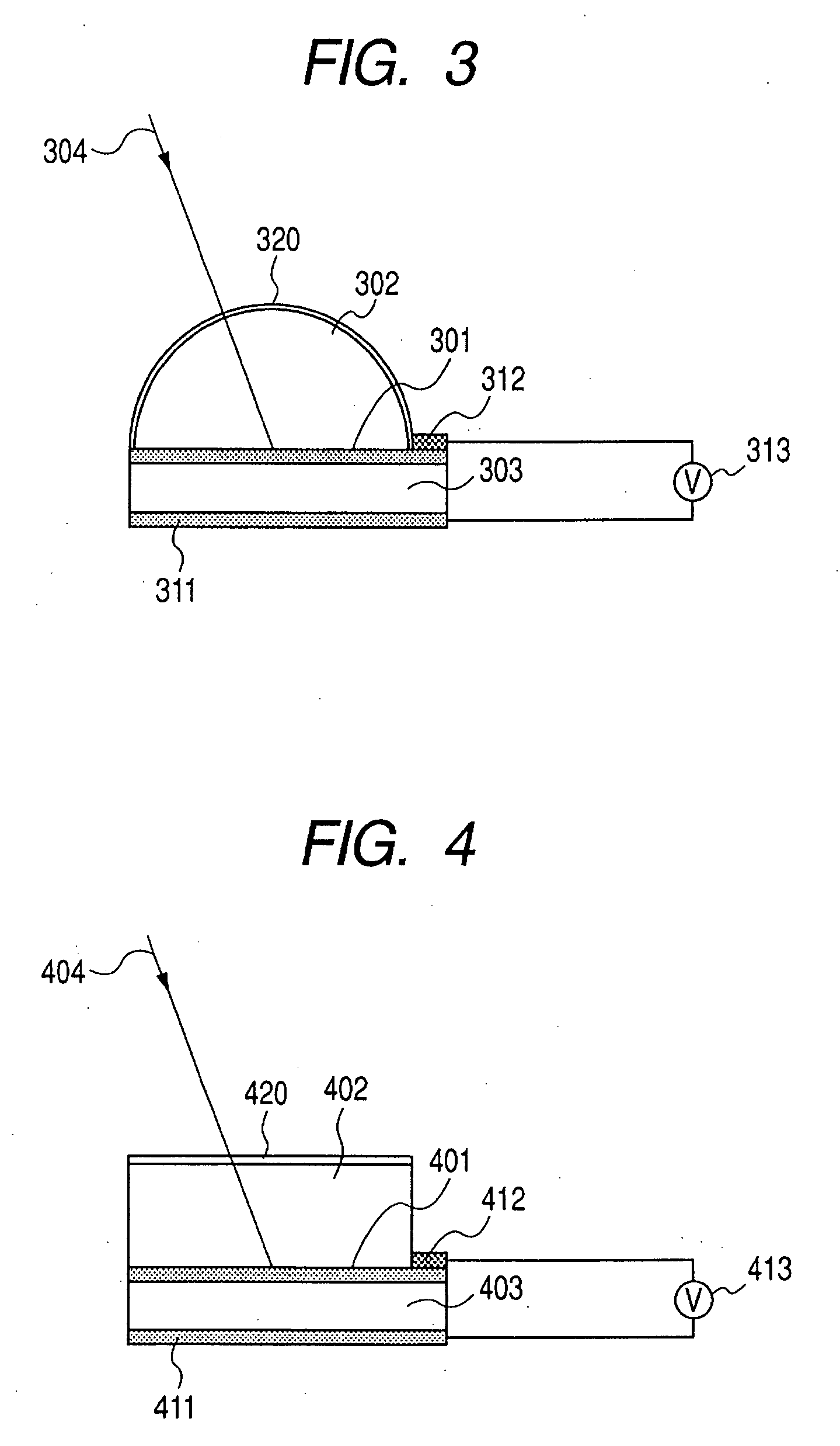
[0041]FIG. 3 is a cross-sectional view illustrating an example of a configuration of a detection device and a filter according to the present invention. In FIG. 3, n-InAs 301 has a dielectric constant with a negative real part in a frequency region including the millimeter wave band up to the terahertz band. Titania ceramics 302 is well known as high-k material in the same frequency region. A DLaTGS crystal 303 is known as a pyroelectric device in the same frequency region. In addition, electrodes 311, 312 work to extract spontaneous polarization of the DLaTGS crystal involved with detection in form of voltage. Therefore, a voltage detector 313 is provided. Further, the voltage detector 313 may include an impedance matching circuit (e.g., a source follower circuit).

[0042]The configuration is the Kretschmann configuration such as shown in FIG. 3, and as described above, from the incidence side of an electromagnetic wave 304 desired to be detected in the range of the millimeter wave b...

example 2

[0048]FIG. 4 is a cross-sectional view illustrating an example of a configuration of a detection device and a filter according to the present invention. In FIG. 4, ITO (In2O3—SnO2) 401 has a dielectric constant with a negative real part in a frequency region including the mid-infrared region to the near-infrared region. Si (undoped) 402 is comparatively transparent, high refractive index material in a frequency region of a wavelength not smaller than 1μm. A LiTaO3 crystal 403 is known as a pyroelectric device in the same frequency region. In addition, electrodes 411, 412 work to extract spontaneous polarization of the LiTaO3 crystal involved with detection in form of voltage. Therefore, a voltage detector 413 is provided. Further, the voltage detector 413 may include an impedance matching circuit (e.g., a source follower circuit).

[0049]The configuration is the Kretschmann configuration such as shown in FIG. 4, and as described above, from the incidence side of an electromagnetic wav...

example 3

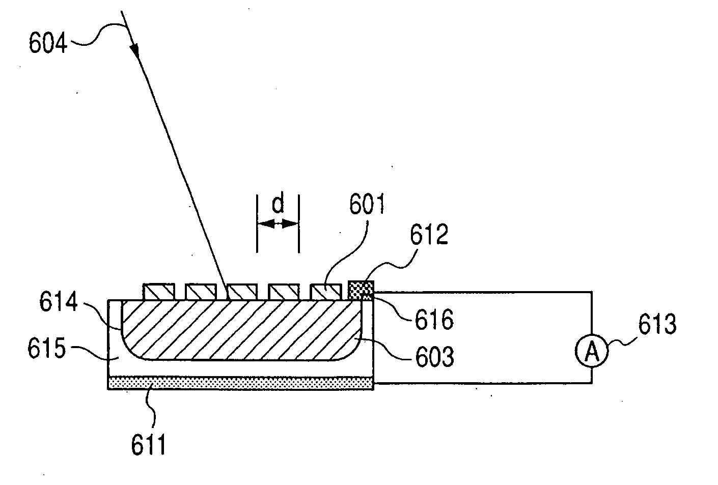
[0052]FIG. 5 is a cross-sectional view illustrating an example of a configuration of a detection device and a filter according to the present invention. In FIG. 5, Au 501 has a dielectric constant with a negative real part in a frequency region including the near-infrared region to the visible region. Si (undoped) 502 is comparatively transparent, high refractive index material in a frequency region of a wavelength not smaller than 1 μm. An InGaAs PIN photodiode 503 is known as a PIN photodiode which supports the same frequency region by varying the mixing ratio of mixed crystal such as In or Ga. For example, In53Ga47As which is lattice-matched to an InP substrate has a peak value of D* in a band of 1.5 μm, which is 1010 cm·Hz1 / 2 / w. A p-type region and an n-type region of the InGaAs PIN photodiode are denoted by 514 and 515, respectively. An i-type region exists between the p-type region 514 and the n-type region 515 but is not shown. An insulating film is denoted by 516. Electrodes...


PUM

PropertyMeasurementUnit
dielectric constantaaaaaaaaaa
thicknessaaaaaaaaaa
thicknessaaaaaaaaaa

Abstract

There is a need for a detection device which has high photoreceptive sensitivity in a generally wide frequency region including the infrared region. Therefore, in the present invention, by utilizing a phenomenon in which electric field strength is enhanced by surface plasmon resonance in a negative dielectric constant medium, a detection device is provided which has an electromagnetic wave detection portion disposed at a position where the electric field strength is large.

Description

BACKGROUND OF THE INVENTION[0001]1. Field of the Invention[0002]The present invention relates to a detection device for detecting an electromagnetic wave of a generally wide frequency region including the infrared region and ranging between a longer wavelength region of the millimeter wave region to the terahertz bandwidth (30 GHz to 30 THz) and a shorter wavelength region of the visible light region, and to an image forming device using the detection device.[0003]2. Description of the Related Art[0004]As a detection device in the infrared region, there have hitherto been widely known a thermal detection device having no wavelength dependency and a quantum detection device having wavelength dependency. Most of these devices utilize a feature of infrared detection. For example, these are applied in a wide range of fields and various applications such as a human body detector at an automatic door, a temperature sensor in a fire alarm or air conditioner, a gas detector using an infrare...

Claims


Application Information

Patent Timeline
Patent Type & Authority Applications(United States)
IPC IPC(8): G01J5/02G01J1/02G01J1/04G01J3/18G01J3/36G01N21/27G01N21/41
CPCG01J1/42H01L27/14621H01L31/0232H01L31/02162H01L27/14627
Inventor SEKIGUCHI, RYOTAOUCHI, TOSHIHIKO
Owner CANON KK
Why Eureka
Try Eureka