Light-emitting device, method for driving the same, and electronic apparatus

a technology of light-emitting devices and electronic devices, which is applied in static indicating devices, instruments, non-linear optics, etc., can solve the problems of significantly reducing the display quality, difficult to measure the temperature of light-emitting elements with high accuracy, and organic el materials used for light-emitting elements

Active Publication Date: 2007-09-20
ELEMENT CAPITAL COMMERCIAL CO PTE LTD
View PDF10 Cites 22 Cited by
  • Summary
  • Abstract
  • Description
  • Claims
  • Application Information

AI Technical Summary

Benefits of technology

[0016] As described above, in the light-emitting device according to the first aspect of the invention, the temperature of the temperature-detection light-emitting element provided in the display area is detected, and the electric current corrected in accordance with the detected temperature is applied to the display light-emitting elements, whereby high-quality image display can be achieved. In particular, since the temperature detector detects the temperature of the temperature-detection light-emitting element by utilizing the temperature characteristic of the temperature-detection light-emitting element provided in the display area, the temperature detection can be implemented within the display area, and a complicated manufacturing process is substantially not necessary.

Problems solved by technology

It is generally known that organic EL materials used for light-emitting elements in organic EL panels, which are an example of light-emitting devices, are problematic in that the brightness varies depending on the ambient temperature due to the unique temperature characteristics of the materials.
Especially in RGB-independent-emission panels, the differences in the unique temperature characteristics of the materials can induce a color shift, which significantly lowers the display quality.
This is technically problematic in that it is difficult to measure the temperature of the light-emitting elements with high accuracy.
Supposedly, if the temperature sensors are to be disposed within the display area of the substrate, the substrate may unfavorably need to be given a complicated structure, such as a multilayer structure, or the aperture ratio of the display area may undesirably become reduced.
In particular, providing a temperature sensor in the central region of the substrate is not only difficult in terms of circuit wiring, but can also cause heat generation and heat radiation by the wiring lines.
On the other hand, setting the sensors externally to the luminescence panel will not make the most of the advantages of organic EL panels, such as compact, low-profile, and lightweight features.
When the device is in operation, heat generated as a result of light emission by the display light-emitting elements or heat generated by wiring resistors or semiconductor elements, such as thin film transistors (TFTs), provided in the pixels may possibly cause the temperature of the pixels to change.

Method used


Image

  • Light-emitting device, method for driving the same, and electronic apparatus
  • Light-emitting device, method for driving the same, and electronic apparatus
  • Light-emitting device, method for driving the same, and electronic apparatus

Examples


first embodiment

[0043] An organic EL device and a method for driving the device according to a first embodiment of the invention will be described below with reference to FIGS. 1 to 7.

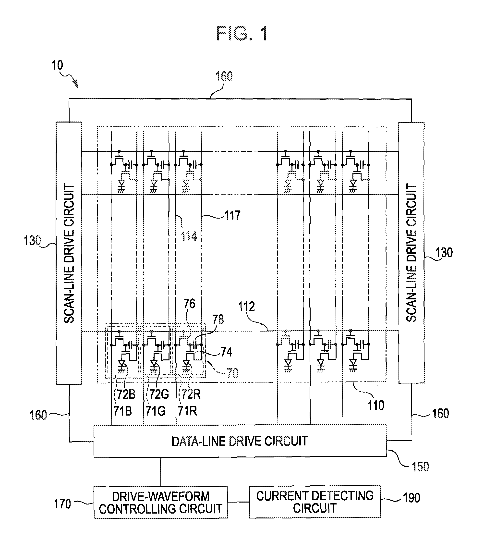
[0044] An overall structure of the organic EL device according to the first embodiment will be described first with reference to FIG. 1. FIG. 1 is a block diagram showing the overall structure of the organic EL device according to the first embodiment.

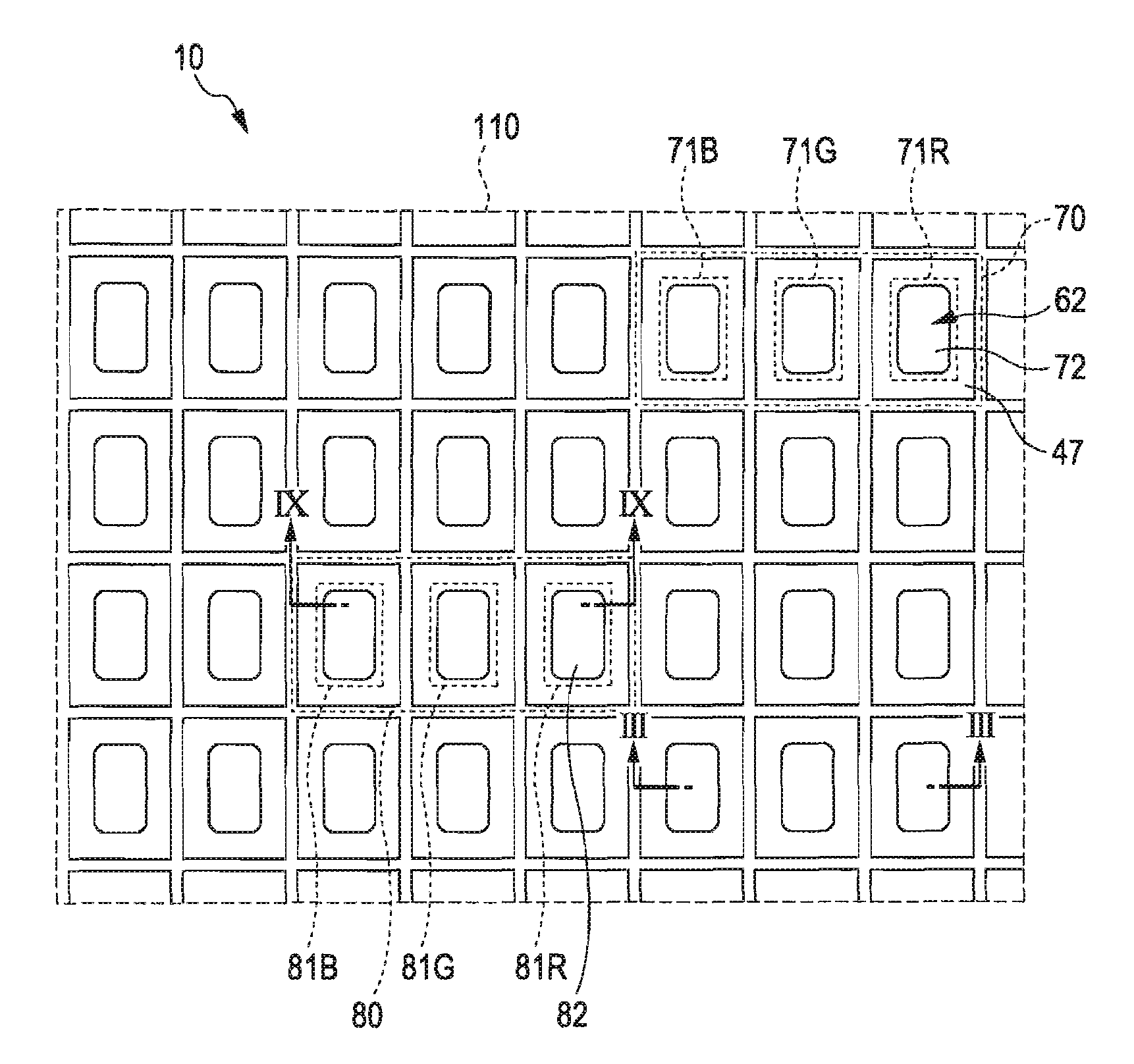
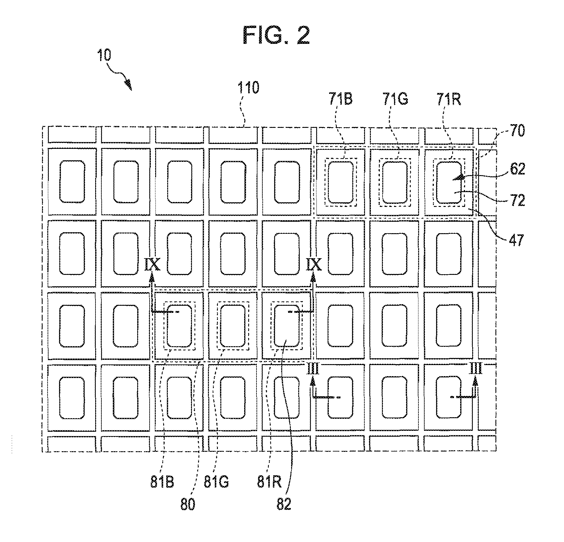
[0045] In FIG. 1 an organic EL device 10 is a display device having built-in drive circuits and driven on the basis of an active matrix driving system. The organic EL device 10 includes pixels 70, each of which is constituted by subpixels 71R, 71G, and 71B.

[0046] The organic EL device 10 has an image display area 110 in which data lines 114 and scan lines 112 are arranged in vertical and horizontal directions, respectively. The subpixels 71R, 71G, and 71B correspond to the intersection points of the data lines 114 and scan lines 112 and are arranged in a matrix. A set...

second embodiment

[0090] An organic EL device and a method for driving the device according to a second embodiment of the invention will be described below with reference to FIGS. 8 and 9. FIG. 8 is a plan view which illustrates the second embodiment and corresponds to the plan view in FIG. 7. FIG. 9 is a block diagram which illustrates the second embodiment and corresponds to the plan view in FIG. 5. In FIGS. 8 and 9, components equivalent to those in the first embodiment shown in FIGS. 1 to 7 are indicated by the same reference numerals, and descriptions of those components will thus be omitted.

[0091] In contrast to the first embodiment in which only the organic EL elements 82GT included in the temperature-detection pixels 80 function as temperature sensors, the subpixels 81R, 81G, and 81B constituting the temperature-detection pixels 80 (i.e. the temperature-detection pixels 80a and 80b) in the second embodiment shown in FIG. 8 have organic EL elements 82RT, 82GT, and 82BT that function as temper...


PUM


Abstract

A light-emitting device includes a plurality of pixels, a temperature-detection pixel, a temperature detector, an applied-current calculator, and a current applying unit disposed on a substrate. The pixels include display light-emitting elements for displaying information. The temperature-detection pixel is provided within a display area where the pixels are disposed and includes a temperature-detection light-emitting element for temperature detection, which is shielded by a light shielding layer and includes the same organic layer as that included in each display light-emitting element. The temperature detector detects a current value of the temperature-detection light-emitting element so as to detect the temperature thereof. The applied-current calculator calculates an electric current to be applied to the display light-emitting elements in accordance with the detected temperature so that the display light-emitting elements emit light with a predetermined luminance. The current applying unit applies the electric current to the display light-emitting elements.

Description

BACKGROUND [0001] 1. Technical Field [0002] The present invention relates to light-emitting devices, such as organic electroluminescence (EL) panels, methods for driving such light-emitting devices, and electronic apparatuses equipped with such light-emitting devices. [0003] 2. Related Art [0004] It is generally known that organic EL materials used for light-emitting elements in organic EL panels, which are an example of light-emitting devices, are problematic in that the brightness varies depending on the ambient temperature due to the unique temperature characteristics of the materials. Especially in RGB-independent-emission panels, the differences in the unique temperature characteristics of the materials can induce a color shift, which significantly lowers the display quality. The term “color shift” refers to a change (shift) in the current-versus-light output characteristic caused by temperature differences occurring within a substrate plane (that is, among pixels in the centra...

Claims


Application Information

Patent Timeline
Patent Type & Authority Applications(United States)
IPC IPC(8): H01L33/00G09G3/20G09G3/30H01L51/50H05B44/00
CPCG09G3/3225G09G2320/041H01L27/3272H01L27/3244H01L27/3211H10K59/35H10K59/126H10K59/12G02F1/1335
Inventor MITSUHASHI, ETSUO
Owner ELEMENT CAPITAL COMMERCIAL CO PTE LTD
Why Eureka
Try Eureka