Method of fabricating local interconnects on a silicon-germanium 3D CMOS

Active Publication Date: 2007-09-20
MICROSOFT TECH LICENSING LLC +1
View PDF1 Cites 180 Cited by
  • Summary
  • Abstract
  • Description
  • Claims
  • Application Information

AI Technical Summary

Benefits of technology

[0006] It is an object of the method of the invention to provide an eas

Problems solved by technology

The interconnection between the silicon CMOS

Method used


Image

  • Method of fabricating local interconnects on a silicon-germanium 3D CMOS
  • Method of fabricating local interconnects on a silicon-germanium 3D CMOS
  • Method of fabricating local interconnects on a silicon-germanium 3D CMOS

Examples


Example

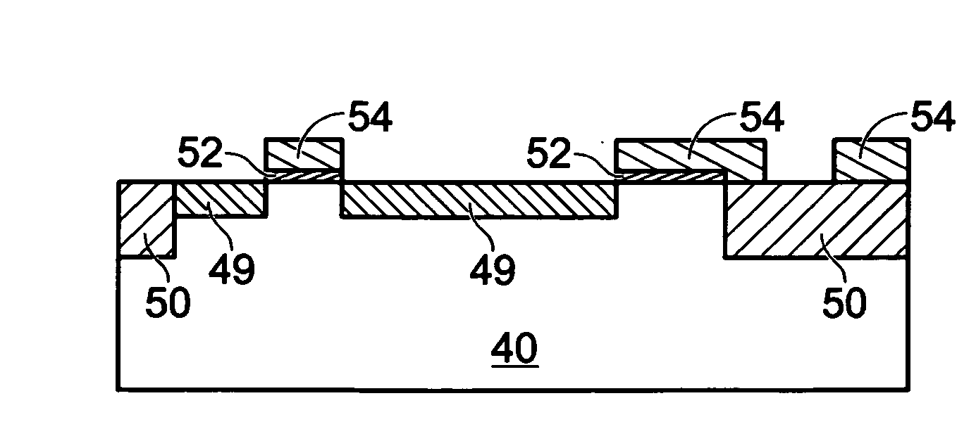
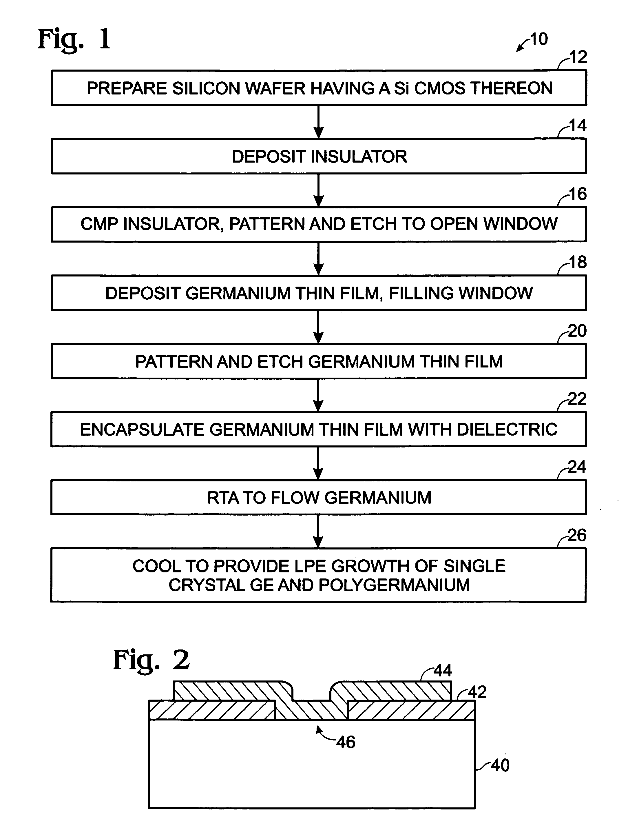
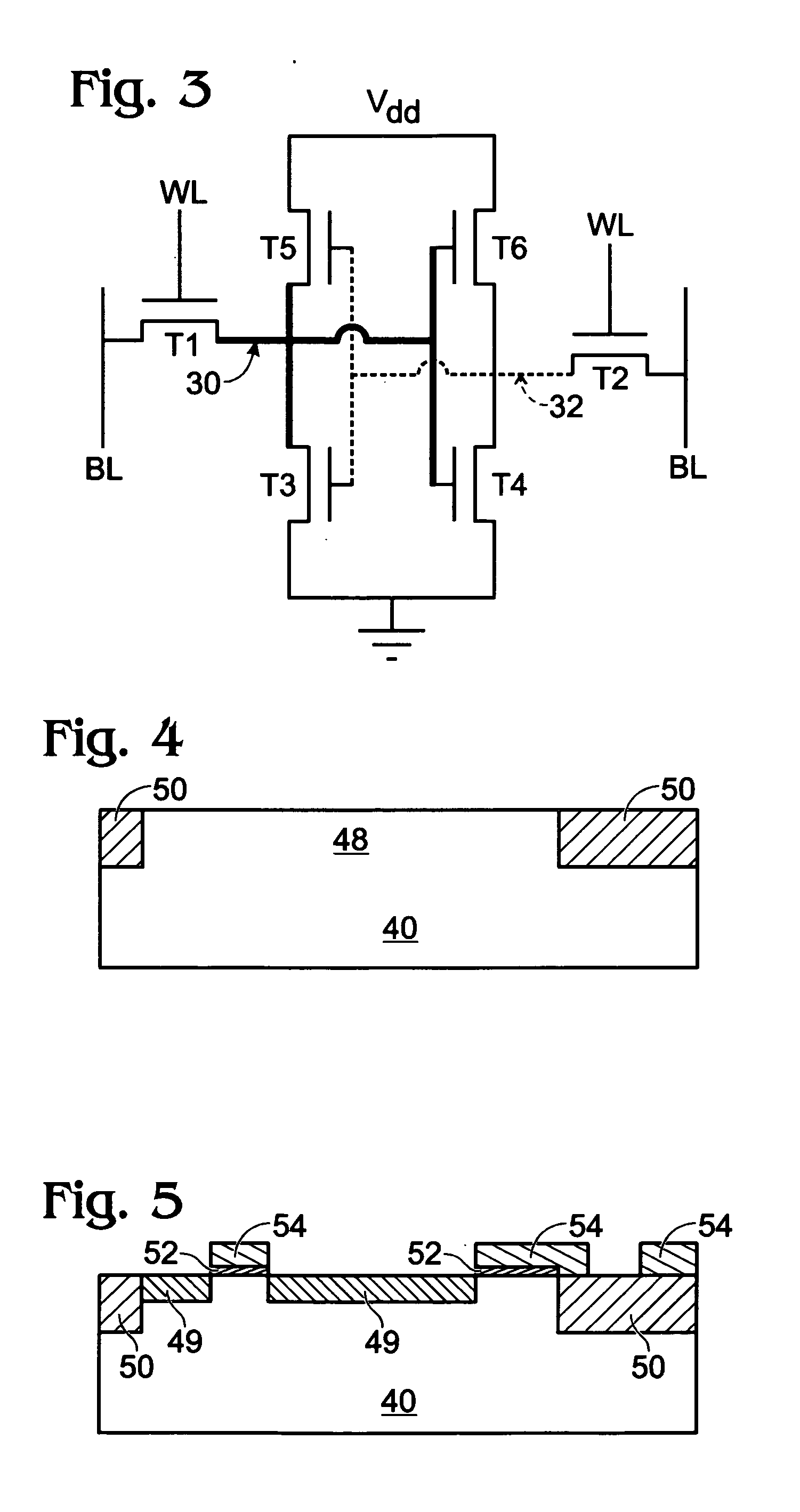
[0013] Interconnects for silicon / silicon 3D devices are usually formed by fabricating metal wires which extend through wafer via holes formed in a wafer in stacked devices which are formed on a plural wafers. The method of the invention uses liquid phase epitaxial germanium growth, which provides, in a seeding area where germanium is in direct contact with silicon, a local interconnect between a silicon CMOS and a germanium CMOS.

[0014] Referring to FIG. 1, a generalized method of the invention is depicted generally at 10. Depending on the nature of the device being fabricated, not all of the steps of the generalized method of the invention are required. A silicon wafer, including any number of silicon-based CMOS devices, is prepared, step 12. A thin layer of insulating material, such as silicon oxide or silicon nitride, having a thickness of between about 500 nm and 1000 nm, is deposited, step 14, onto the silicon wafer. The insulator layer may be a single insulator layer, or may b...


PUM


Abstract

A method of fabricating local interconnect on a silicon-germanium 3D CMOS includes fabricating an active silicon CMOS device on a silicon substrate. An insulator layer is deposited on the silicon substrate and a seed window is opened through the insulator layer to the silicon substrate and to a silicon CMOS device gate. A germanium thin film is deposited on the insulator layer and into windows, forming a contact between the germanium thin film and the silicon device. The germanium thin film is encapsulated in a dielectric material. The wafer is heated at a temperature sufficient to flow the germanium, while maintaining the other layers in a solid condition. The wafer is cooled to solidify the germanium as single crystal germanium and as polycrystalline germanium, which provides local interconnects. Germanium CMOS devices may be fabricated on the single crystal germanium thin film.

Description

FIELD OF THE INVENTION [0001] This invention relates to high speed integrated circuits, and specifically to a method for fabrication of a germanium CMOS device on a silicon CMOS device and other 3D CMOS devices. BACKGROUND OF THE INVENTION [0002] Known silicon-germanium CMOS structures are fabricated above, or on, a conventional silicon CMOS, and a dielectric layer is provided to separate the convention silicon CMOS from the germanium CMOS. The interconnection between the silicon CMOS and germanium CMOS is difficult to fabricate. This invention provides a local interconnect between the silicon CMOS and germanium CMOS that can significantly increase the device density. [0003] Liu et al., High quality single-crystal Germanium on insulator by liquid-phase epitaxy on Silicon substrate, Applied Physics Letters, vol. 84, no. 14, pp 2563-2565. SUMMARY OF THE INVENTION [0004] A method of fabricating local interconnect on a silicon-germanium 3D CMOS includes fabricating an active silicon CMO...

Claims


Application Information

Patent Timeline
IPC IPC(8): H01L21/8238
CPCH01L21/02532H01L21/02667H01L21/28525H01L27/1108H01L21/823871H01L27/11H01L21/76895H10B10/00H10B10/125
Inventor LEE, JONG-JANSCHUELE, PAUL J.HSU, SHENG TENGMAA, JER-SHEN
Owner MICROSOFT TECH LICENSING LLC
Why Eureka
Try Eureka