System and apparatus for designing layout of a LSI

a technology of layout and system, applied in the direction of cad circuit design, program control, instruments, etc., can solve the problems of inability to achieve sufficient effect of power dissipation reduction, the length of the effective interconnect for reducing power dissipation is likely to increase, etc., to achieve the effect of reducing power dissipation

Inactive Publication Date: 2007-09-20
NEC CORP
View PDF4 Cites 9 Cited by
  • Summary
  • Abstract
  • Description
  • Claims
  • Application Information

AI Technical Summary

Benefits of technology

[0007]It is an object of the present invention to provide a layout design apparatus, a method thereof, and a program thereof which are capable of achieving a layout that can reduce the power dissipation while satisfying the ti g constraint in a single layout modification process.

Problems solved by technology

In such a case, when the error correction is performed using only the timing as criterion, even though there is a solution satisfying both the timing and the reduction in the power dissipation, the length of the interconnect effective for reducing the power dissipation is likely to increase, with the result that a sufficient effect of reduction in the power dissipation cannot be obtained.

Method used


Image

  • System and apparatus for designing layout of a LSI
  • System and apparatus for designing layout of a LSI
  • System and apparatus for designing layout of a LSI

Examples


Embodiment Construction

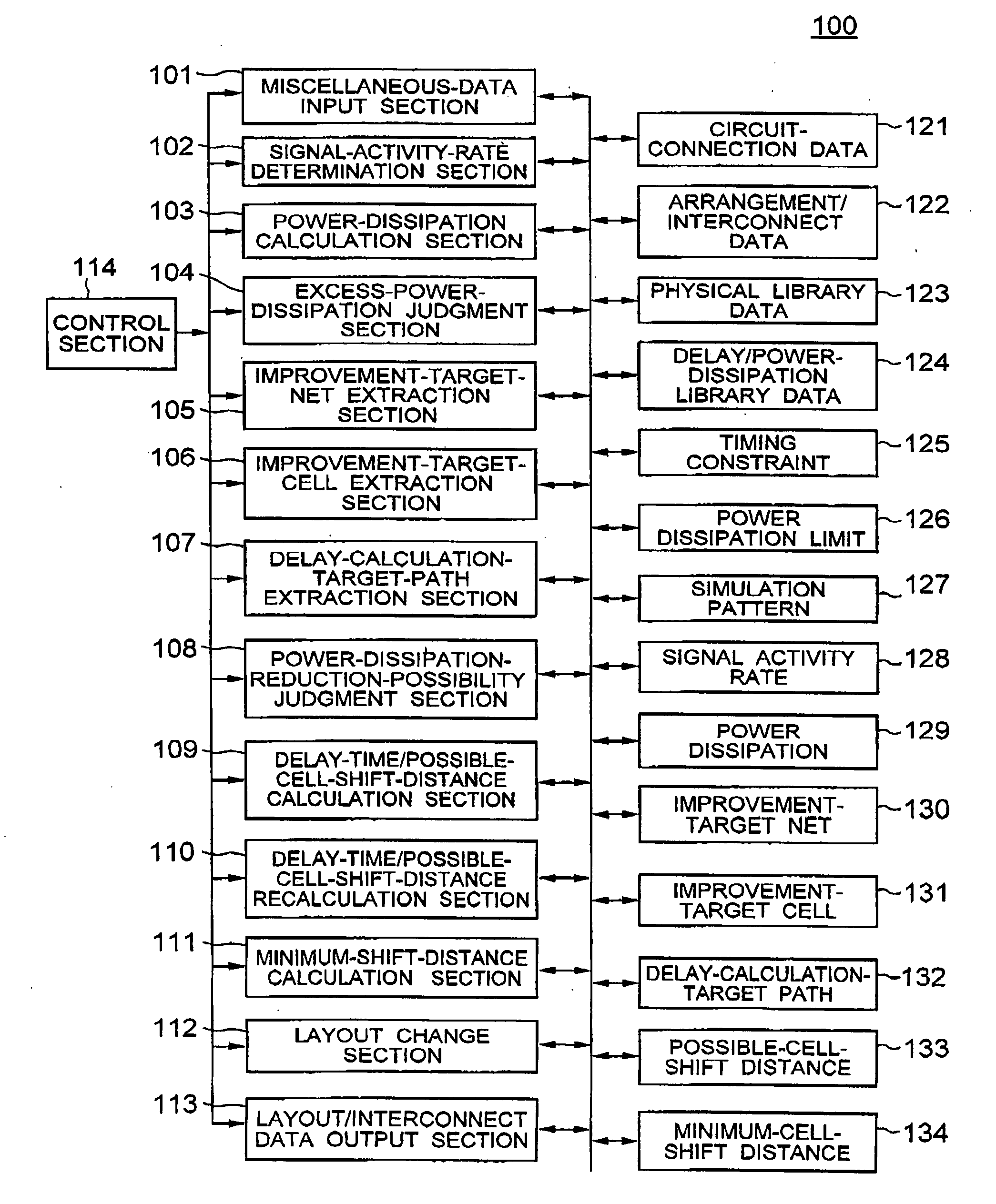
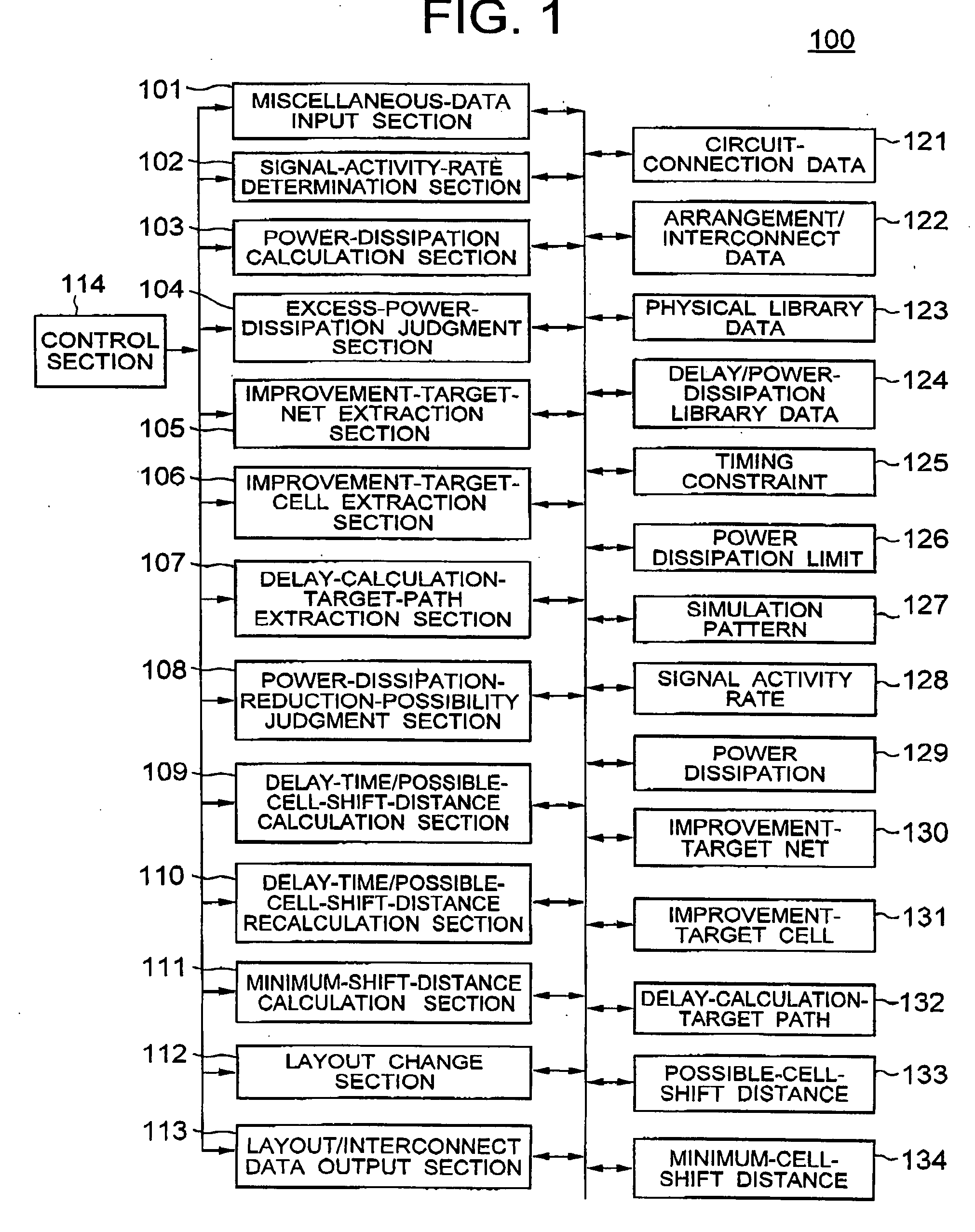
[0028]An embodiment of the present invention will be described in detail below with reference to the accompanying drawings. FIG. 1 shows the configuration of a layout design apparatus according to an embodiment of the present invention. The layout design apparatus 100 shown in FIG. 1 includes a miscellaneous-data input section 101, a signal-activity-rate determination section 102, a power-dissipation calculation section 103, an excess-power-dissipation judgment section 104, an improvement-target-net extraction section 105, an improvement-target-cell extraction section 106, a delay-calculation-target-path extraction section 107, a power-dissipation-reduction-possibility judgment section 108, a delay-time / possible-cell-shift-distance calculation section 109, a delay-time / possible-cell-shift-distance recalculation section 110, a minimum-shift-distance calculation section 111, a layout change section 112, an layout / interconnect data output section 113, and a control section 114. The lay...


PUM


Abstract

A judgment section determines whether or not a reduction in the power dissipation is possible by relocation of an improvement-target cell. If a reduction in the power dissipation is possible, a calculation section calculates the delay time of a target path including the improvement-target cell to obtain a possible shift distance of the improvement-target cell, within which the timing constraint is satisfied. A layout change section relocates the improvement-target cell within a range in which the power dissipation can be reduced and timing constraint can be satisfied.

Description

BACKGROUND OF THE INVENTION[0001]1. Field of the Invention[0002]The present invention relates to a system and an apparatus for designing layout of a LSI (large-scale-integrated circuit).[0003]2. Description of the Related Art[0004]A computer-aided design (CAD) system is often used in designing a semiconductor device such as a LSI. In the designing process using the CAD system, automatic layout design is performed based on the arrangement of circuits or information concerning connection between circuits to thereby determine the positions of respective circuits or interconnection route between circuits on the semiconductor device. After completion of the layout design, verification is made to ascertain whether or not the timing constraint between circuits is satisfied or whether or not power dissipation falls within the predetermined limit in the designed layout. If it has been determined that the timing constraint between circuits is not satisfied or that the power dissipation does n...

Claims


Application Information

Patent Timeline
Patent Type & Authority Applications(United States)
IPC IPC(8): G06F17/50G06F9/455
CPCG06F2217/78G06F17/5068G06F30/39G06F2119/06
Inventor GOTO, TAKASHI
Owner NEC CORP
Why Eureka
Try Eureka