
Method for patterning a photovoltaic device comprising CIGS material using an etch process

a photovoltaic device and etching technology, applied in the direction of pv power plants, light radiation electric generators, generators/motors, etc., can solve the problems of limited wiring means of photovoltaic modules, limited module efficiency, and wide scribes, etc., to achieve better and more efficient photovoltaic modules and high selectivity

Inactive Publication Date: 2007-10-04
APPLIED MATERIALS INC
View PDF16 Cites 106 Cited by
  • Summary
  • Abstract
  • Description
  • Claims
  • Application Information

AI Technical Summary

Benefits of technology

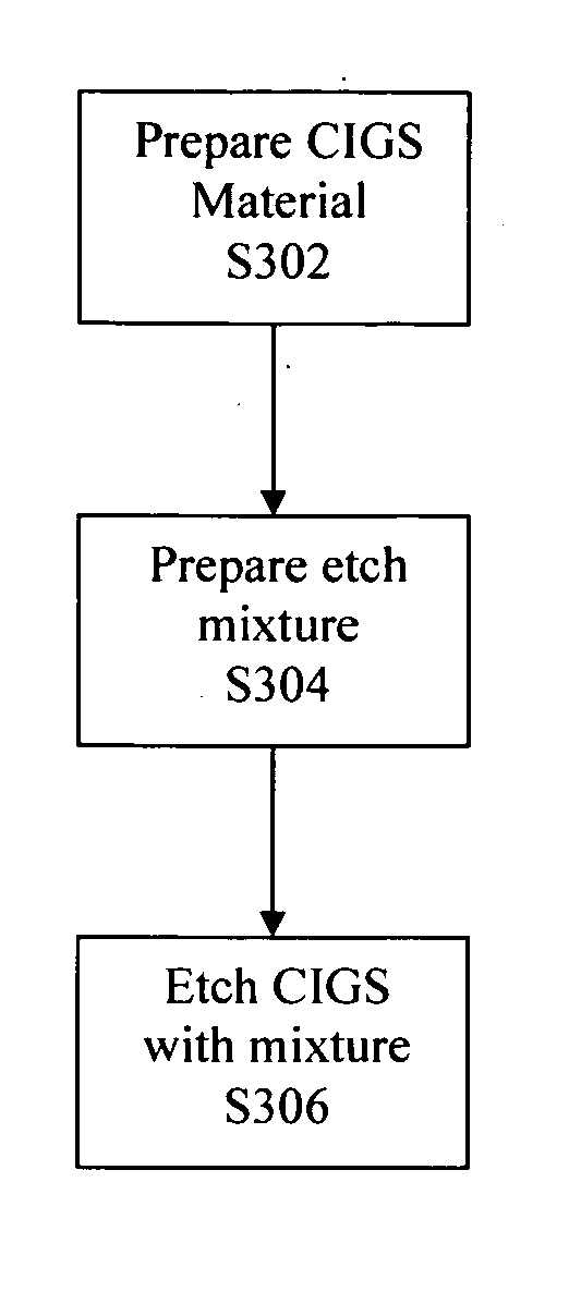
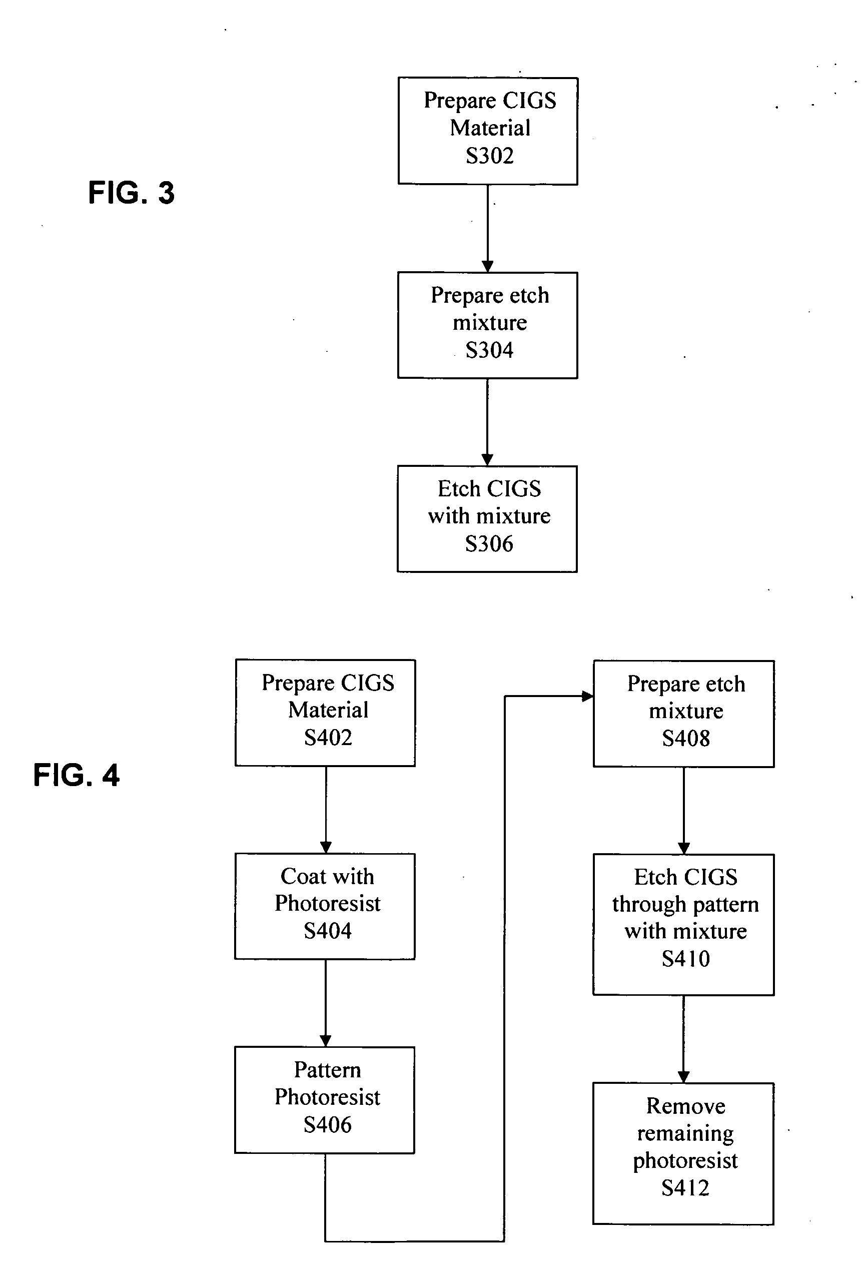
[0015] The present invention provides a method of patterning a thin-film photovoltaic module into cells and / or sub-cells using an etch process. According to one aspect, an etch mixture is identified that is capable etching through a thin-film material such as CIGS with high selectivity to both photoresist and underlying layers such as metal. According to another aspect, the etch process enables patterning a photovoltaic device using lithographic techniques. Among other things, the invention enables forming interconnect structures with feature sizes that are substantially smaller than is possible with prior art techniques, and avoids many of the problems associated with laser and mechanical scribes, thus resulting in better and more efficient photovoltaic modules.

Problems solved by technology

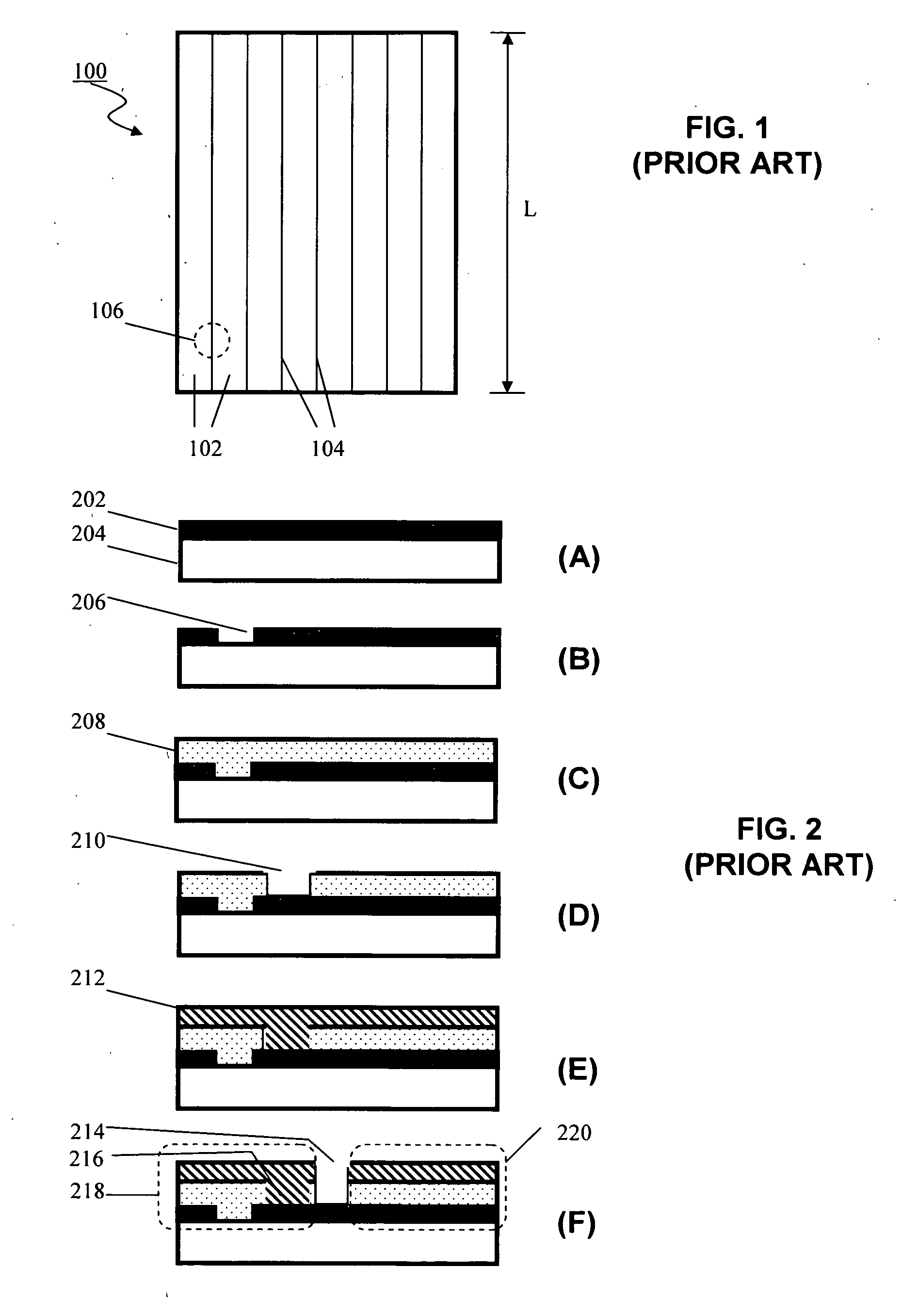
The prior art patterning processes using laser and mechanical scribing such as that described above has a number of drawbacks that limit module efficiency.
For example, they create wide scribes, defects, and shunt current paths.
Furthermore, they provide limited means for wiring the module in series-parallel arrangements that might reduce sensitivity to shading losses or non-uniformity.
The literature contains only limited references to performing etches in connection with CIGS material, and these references are limited to specific purposes that are not useful for patterning modules such as finishing the surface of a CIGS layer or reducing surface defects.
In addition to not being useful as a complete etch, it should be noted that use of KCN in production may be impractical because of safety considerations associated with the high toxicity of this substance.
As should be apparent, none of these conventional processes are useful for etching or patterning a thin film CIGS layer, which requires rapidly etching completely through two or more microns of CIGS, as opposed to a surface treatment which slowly removes a few angstroms from the surface.
In addition to surface treatments, other conventional processes cannot obtain a CIGS etch useful for patterning.
Also, throughput is limited for long grooves, as are used to isolate cells in modules.

Method used


Image

  • Method for patterning a photovoltaic device comprising CIGS material using an etch process
  • Method for patterning a photovoltaic device comprising CIGS material using an etch process
  • Method for patterning a photovoltaic device comprising CIGS material using an etch process

Examples


Embodiment Construction

[0053] The present invention will now be described in detail with reference to the drawings, which are provided as illustrative examples of the invention so as to enable those skilled in the art to practice the invention. Notably, the figures and examples below are not meant to limit the scope of the present invention to a single embodiment, but other embodiments are possible by way of interchange of some or all of the described or illustrated elements. Moreover, where certain elements of the present invention can be partially or fully implemented using known components, only those portions of such known components that are necessary for an understanding of the present invention will be described, and detailed descriptions of other portions of such known components will be omitted so as not to obscure the invention. In the present specification, an embodiment showing a singular component should not be considered limiting; rather, the invention is intended to encompass other embodime...


PUM


Abstract

A processing method herein enables patterning a thin-film photovoltaic module into cells and / or sub-cells using an etch process. According to one aspect, an etch mixture is identified that is capable etching through a thin-film material such as CIGS with high selectivity to both photoresist and underlying layers such as metal. According to another aspect, the etch process enables patterning a photovoltaic device using lithographic techniques. Among other things, the invention enables forming interconnect structures with feature sizes that are substantially smaller than is possible with prior art techniques, and avoids many of the problems associated with laser and mechanical scribes, thus resulting in better and more efficient photovoltaic modules.

Description

FIELD OF THE INVENTION [0001] The present invention relates generally to photovoltaic devices, and more particularly to a method for etching CIGS material in a manner that is suitable for application in patterning a photovoltaic module comprising a CIGS material. BACKGROUND OF THE INVENTION [0002] Thin layers of material comprising Cu(In,Ga)Se, i.e. CIGS, are known to exhibit the highest photovoltaic conversion efficiency of any thin film material for a photovoltaic device (19.5%). Consequently, this is an attractive material for use in the manufacture of thin film photovoltaic panels. [0003] In prior art processes, panels containing CIGS material are patterned to form a series-connected chain of cells in order to reduce the current. For example, a 1 m2 panel at 12% efficiency would provide 120 watts of power. If the cell operating voltage is 0.6 volts, then the current is 200 amps, far in excess of what could be carried in the thin films used to contact the front and back of the ce...

Claims


Application Information

Patent Timeline
IPC IPC(8): H02N6/00
CPCH01L31/0322H01L31/046Y02E10/541H01L31/0463
Inventor PEROZZIELLO, ERICBORDEN, PETER
Owner APPLIED MATERIALS INC
Learn More