
Heat dissipation structure of backlight module

a backlight module and heat dissipation structure technology, applied in lighting and heating apparatus, instruments, semiconductor/solid-state device details, etc., can solve the problems of inability to meet the requirements, the size of the fins required is also increasing, and the heat dissipation structure of the conventional backlight module is too large in size, so as to achieve the effect of small size and low cos

Active Publication Date: 2007-10-04
AU OPTRONICS CORP
View PDF5 Cites 29 Cited by
  • Summary
  • Abstract
  • Description
  • Claims
  • Application Information

AI Technical Summary

Benefits of technology

[0008] Hence, one aspect of the present invention is to provide a heat dissipation structure of a backlight module, thereby integrating the heat dissipation mechanism into a circuit board for achieving the objectives of small size, low cost and heat conduction.

Problems solved by technology

However, the efficiency and longevity of the LED are dependent on whether the entire backlight module has good heat-dissipation.
However, the fins disposed on the backlight module make the backlight module too big, and especially, when the power of the LED is increasing, the sizes of the fins required therefore are also increasing.
Hence, the heat dissipation structure of the conventional backlight module is too big in size and cannot satisfy the requirements of the products developed towards lightness and smallness,
Besides, the aluminum substrate is quite expensive and cannot be combined with a circuit board as a multi-layered substrate, thus increasing the product fabrication cost and the design difficulty level.
Moreover, the conventional skill does not implement electrical isolation between the heat-dissipating and electrically conductive paths of the backlight module, thus likely causing a short circuit resulting in damage on the LCD.

Method used


Image

  • Heat dissipation structure of backlight module
  • Heat dissipation structure of backlight module
  • Heat dissipation structure of backlight module

Examples


Embodiment Construction

[0019] Reference will now be made in detail to the preferred embodiments of the present invention, examples of which are illustrated in the accompanying drawings. Wherever possible, the same reference numbers are used in the drawings and the description to refer to the same or like parts.

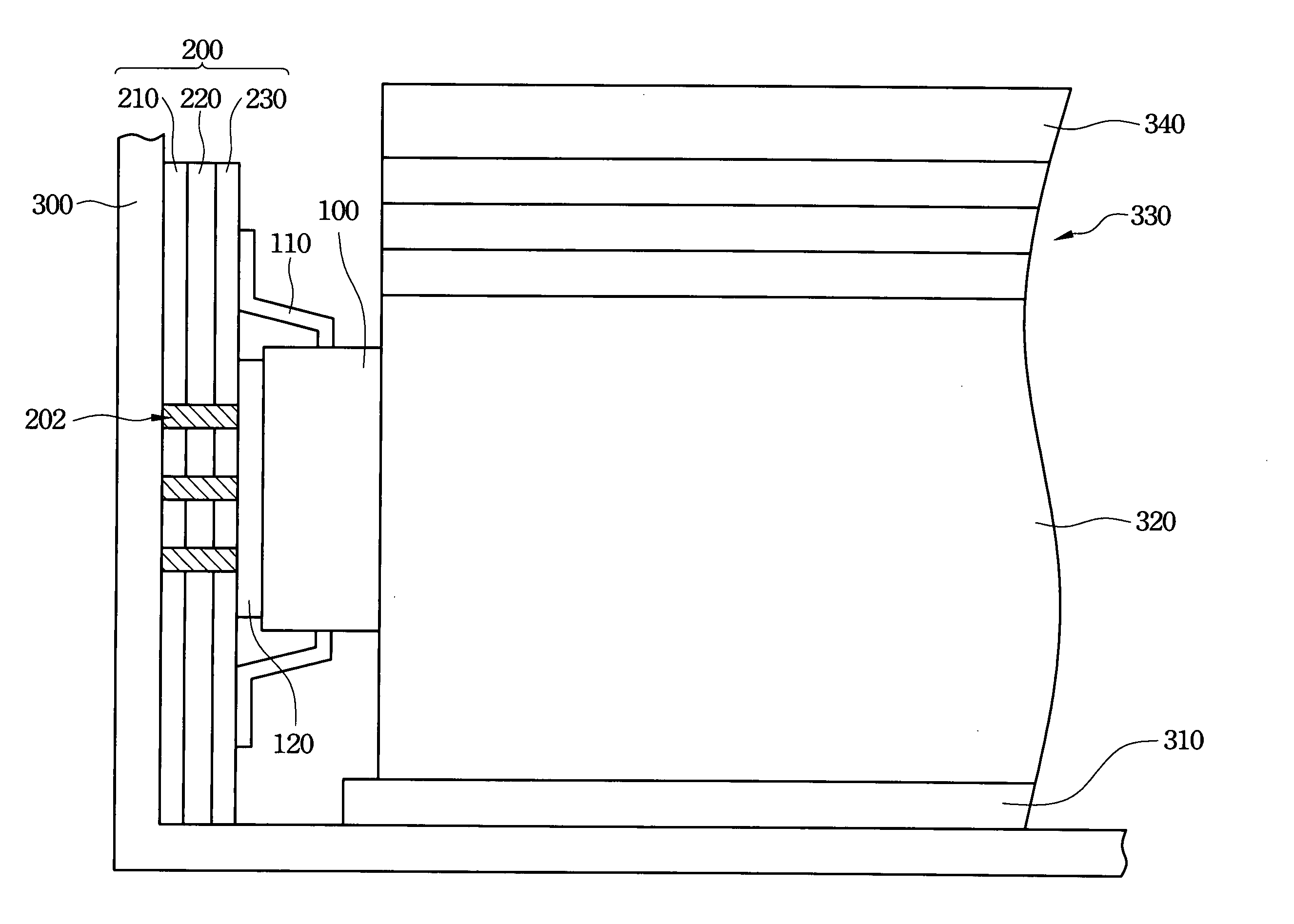
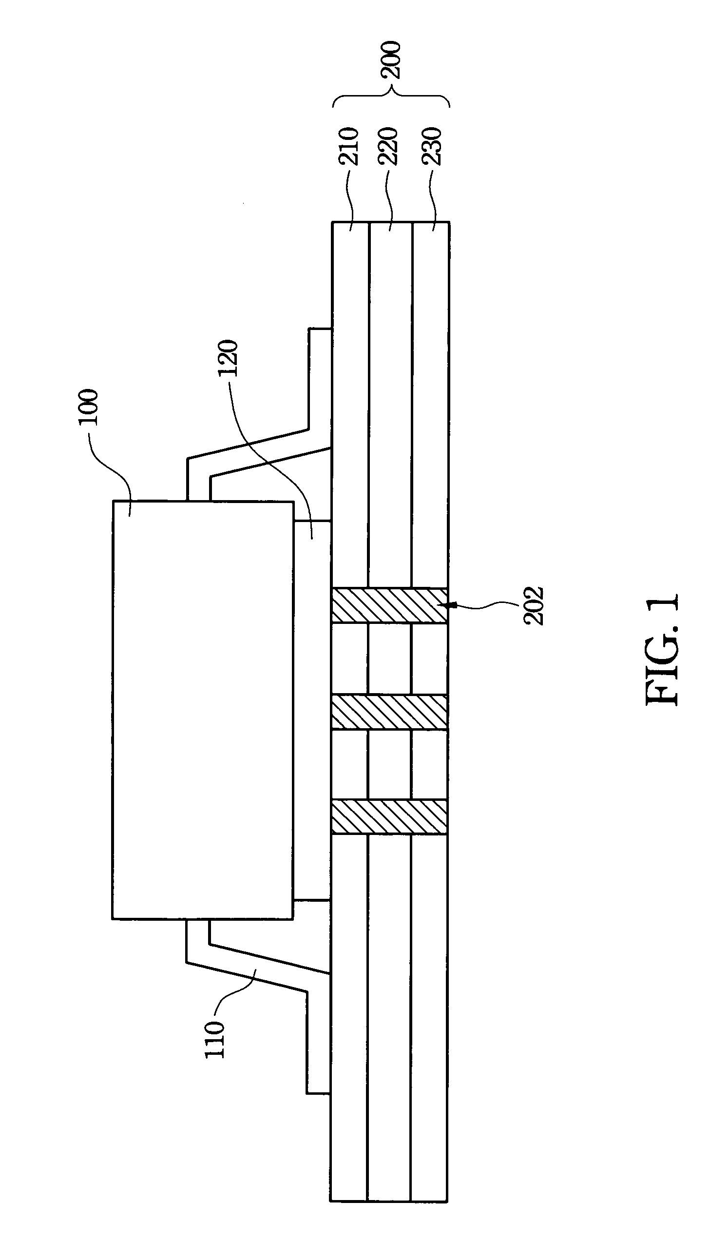
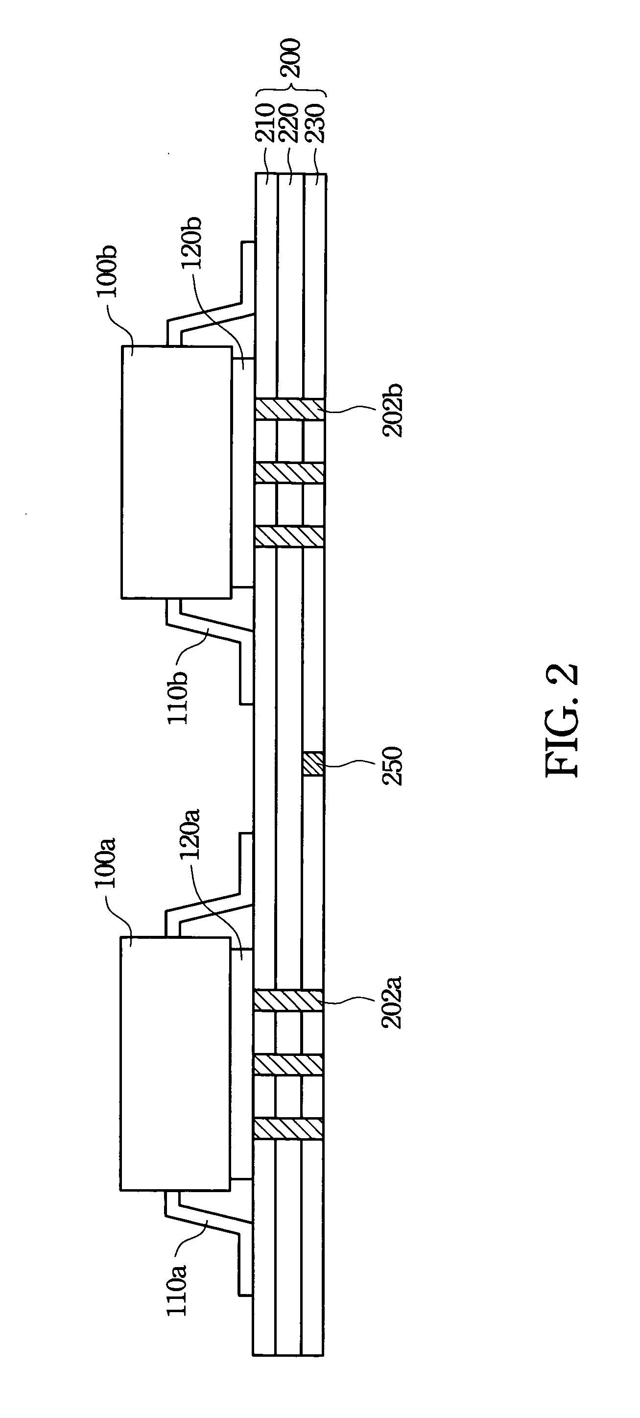
[0020] Referring to FIG. 1, FIG. 1 is a schematic diagram showing a heat-dissipation structure of a backlight module according to a preferred embodiment of the present invention, wherein a circuit board 200 is composed of an electric circuit layer 210, an insulation layer 220 and a heat conductive layer 230, and the electric circuit layer 210 and the heat conductive layer 230 are formed respectively on two opposite surfaces of the circuit board 200 (the insulation layer 220), i.e. the insulation layer 220 is sandwiched between the electric circuit layer 210 and the heat conductive layer 230. The present invention is mainly to implement a plurality of through holes 202 penetrating through the electr...


PUM


Abstract

The heat dissipation structure of the backlight module of the present invention comprises a circuit board, a heat-conductive element (such as thermally conductive glue) and a light-emitting diode (LED) chip, wherein the circuit board has an electric circuit layer and a heat conductive layer respectively formed on two opposite surfaces thereof. The circuit board has a plurality of through holes penetrating through the electric circuit layer and the heat-conductive layer of the circuit board, wherein each of the through holes is filled with heat-conductive material. The heat-conductive element is placed on the circuit layer and covers the through holes, and the LED chip is disposed on the heat-conductive element and is electrically connected to the electric circuit layer.

Description

RELATED APPLICATIONS [0001] The present application is based on, and claims priority from, Taiwan Patent Application Serial Number 95111647, filed on Mar. 31, 2006, the disclosure of which is hereby incorporated by reference herein in its entirety. BACKGROUND [0002] 1. Field of Invention [0003] The present invention relates to a heat dissipation structure of a backlight module. More particularly, the present invention relates to a heat dissipation structure integrated into a circuit board of a backlight module. [0004] 2. Description of Related Art [0005] A backlight module is one of the fundamental parts in a liquid crystal display (LCD). Since liquid crystal does not emit light itself, the backlight module is needed for providing the required light source. A backlight source commonly used in the backlight module can be a cold cathode fluorescent lamp (CCFL) and an LED (Light-Emitting Diode), etc. In comparison with the CCFL used as the backlight source, the LED has the advantages o...

Claims


Application Information

Patent Timeline
IPC IPC(8): G02F1/1333
CPCF21K9/00G02B6/0073G02B6/0085H05K1/0206F21V29/83H05K3/386H05K2201/0209H05K2201/10106F21V29/70H05K3/0061H05K1/118H05K2201/0979
Inventor CHENG, CHI-CHENHO, YA-TINGWU, MENG-CHAI
Owner AU OPTRONICS CORP
Learn More