Application of electronic components in printed products

a technology of electronic components and printed products, applied in the direction of electrical apparatus casings/cabinets/drawers, semiconductor/solid-state device details, instruments, etc., can solve the problems of complex methods, detuning and output losses of rfid elements or transponders, and the need for very precise positioning of chips or chips and auxiliary carriers, etc., to achieve quick and operationally safe application and connection

Inactive Publication Date: 2007-10-04
EVONIK DEGUSSA GMBH +1
View PDF15 Cites 20 Cited by
  • Summary
  • Abstract
  • Description
  • Claims
  • Application Information

AI Technical Summary

Benefits of technology

[0008]In view of the foregoing, a general object of the present invention is to provide a quick and operationally safe application and connection method for electronic components with conductor tracks or antenna structures. Another object of the invention is to provide electronic components and a suitable apparatus for processing such electronic components.
[0010]The absolute positioning of the transponder, which includes at least an antenna and a chip on the printed product, can be varied within tight limits. As is generally known by those skilled in the art, an advantage of RFID or transponder technology is that visual contact with the reading device such as is necessary with a barcode is not required. Thus, the transponder can be placed inside a package. Additionally, with a RFID tag (also referred to as a “smart label”), the absolute position of the transponder within the limits of the tag is not an issue.
[0011]Since the exact application of the chip or auxiliary carrier and chip on an antenna can be considered the most important factor limiting output in a production process, significant advantages can be obtained by simplifying this step. A first approach for simplifying the chip application step is by eliminating the need for precise positioning. Another way to simplify the application process is by eliminating the complicated bonding process using conductive or anisotropic adhesives with long curing times to produce contacts between the chip or the auxiliary carrier and chip.
[0012]According to the invention, the production of a transponder is accelerated by bonding the chip or the auxiliary carrier and chip directly on the material to be printed or the printed product. In such case, the bonding agent only needs to provide sufficient adhesion to the material to be printed or the printed product. After the application of the chip or the auxiliary carrier and chip, the position of the chip or auxiliary carrier and chip is determined by a sensor system, preferably a camera. A printing or stamping system for printing the antenna structure is arranged after the application process and is controlled so that the contacts of the chip or auxiliary carrier are covered with a conductive printing ink or blocking foil so that contact between the chip or the auxiliary carrier and chip and the antenna structure is ensured.
[0013]An important advantage of such an arrangement or process is that the printing or stamping system can be adjusted dynamically in the peripheral, side or diagonal registers so that the antennas are printed or stamped within tight limits at the precise desired angle and position relative to the previously applied chip or chip on an auxiliary carrier. This method can be easily transferred from the production of transponders to other applications that involve connection of an electronic component to a conductor track.
[0014]Due to the very low accuracy required for the positioning of the chip or auxiliary carrier and chip, the application process can be performed significantly more quickly. As a result, higher throughput can be achieved by reducing the production bottleneck at the chip application stage.

Problems solved by technology

The disadvantage of this process is that the chip or chip and auxiliary carrier must be positioned very precisely on the antenna contacts.
It is known that with RFID or transponder technology even a slightly off-center deviation of the chip relative to the antenna during mounting can lead to detuning and output losses of the RFID element or transponder.
Because of the precise positioning that is required, the printed product must be fed in a very accurate manner and a complicated method must be used to position the chip.
A second production rate restriction is that the chip or the auxiliary carrier and chip on this auxiliary carrier must enter into a close connection with the contacts of the antenna.
This significantly slows the process and makes continuous and economical production difficult.
As a result, the chip application process can quickly become a bottleneck for the entire production process.

Method used


Image

  • Application of electronic components in printed products
  • Application of electronic components in printed products
  • Application of electronic components in printed products

Examples


Embodiment Construction

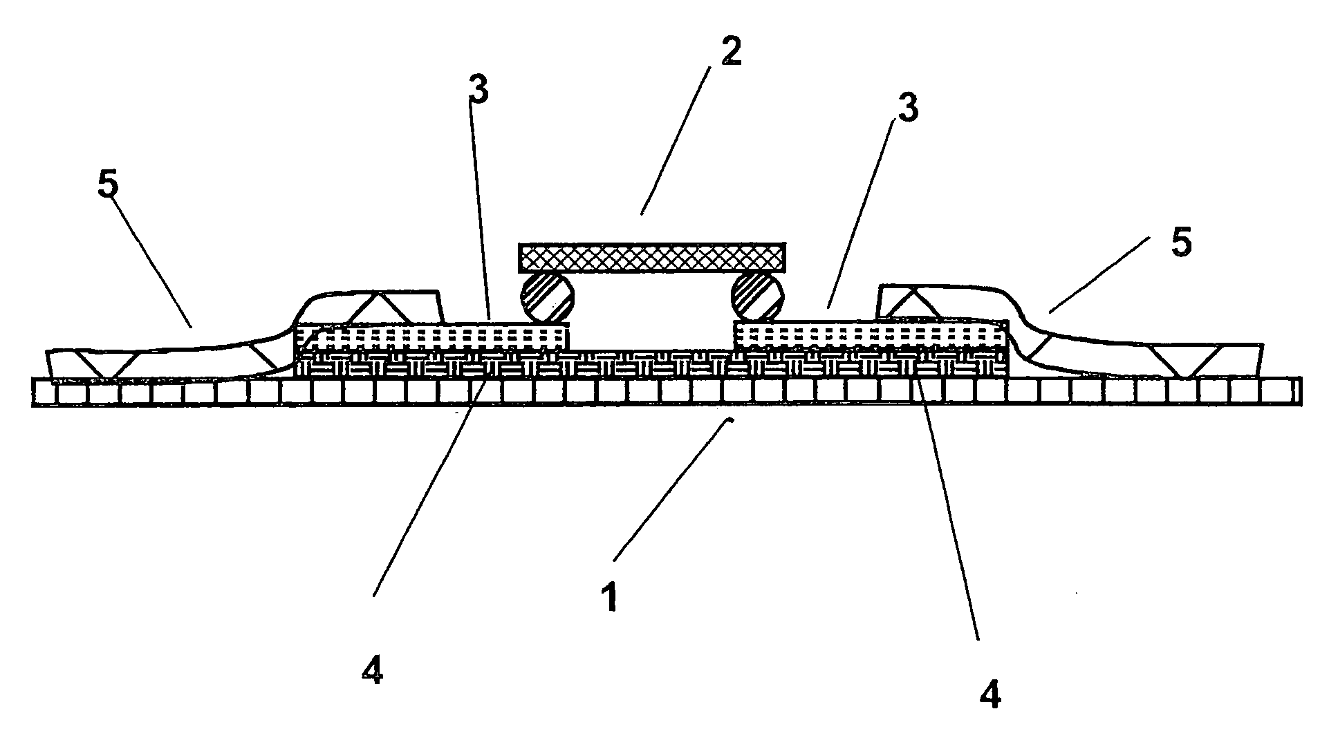
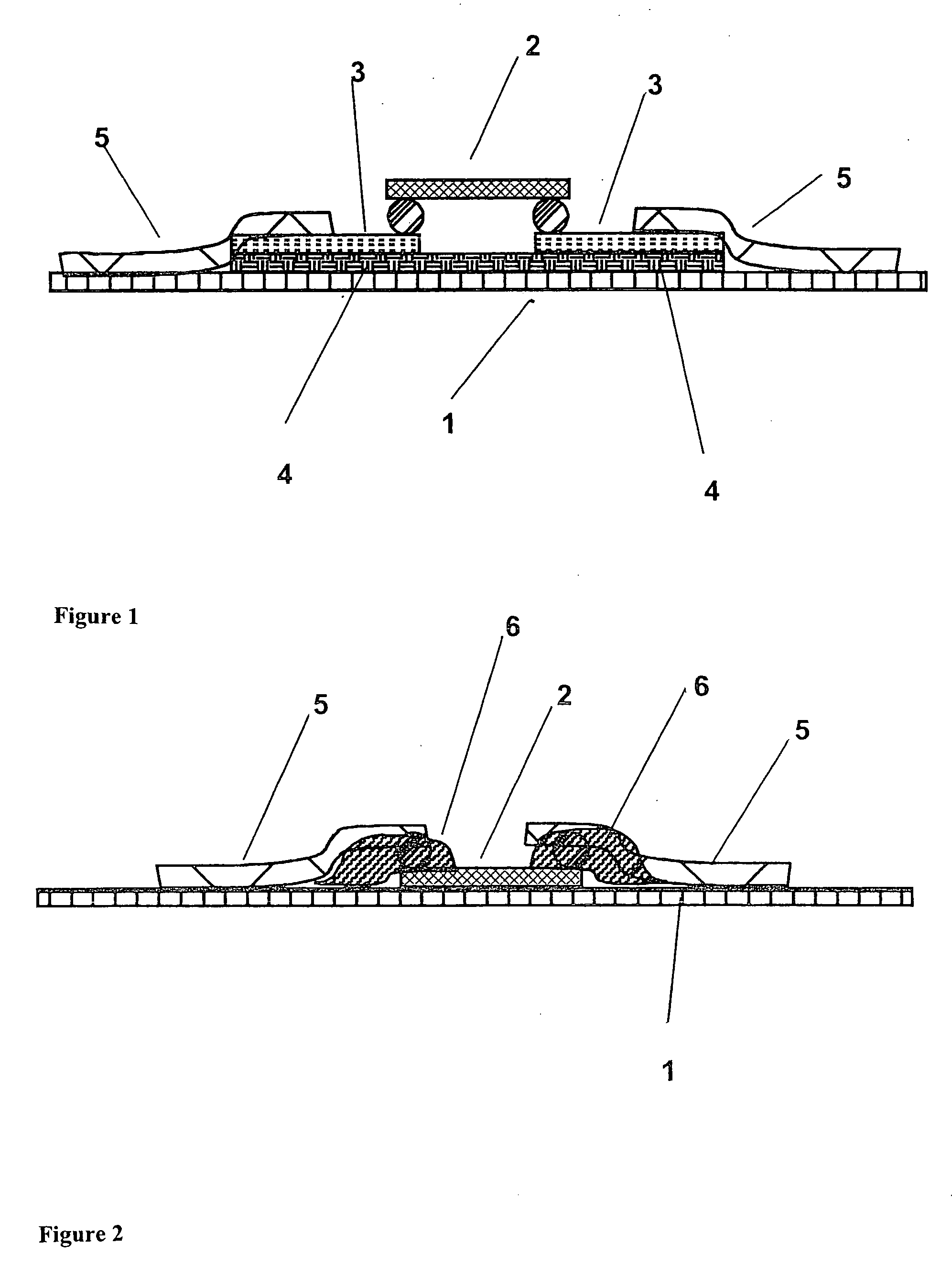
[0022]Referring to FIG. 1 of the drawings, an auxiliary carrier 4 is shown that has been fixed on a printing material or material to be printed 1 using a bonding agent or some other suitable method. The auxiliary carrier 4 has conductive contact areas 3 that are in contact with the contact areas of a chip 2. In a second processing step, conductive structures 5, which in this case are components of an antenna of an RFID transponder, have been printed or stamped over the contact areas 3 of the auxiliary carrier 4. It is significant that, in contrast to the typical procedure, the contact areas are located not on the print side, but instead on the side of the auxiliary carrier and chip facing away from the print side in order to allow printing.

[0023]An arrangement of an individual chip (i.e., which is not located on an auxiliary carrier) on material to be printed 1 is shown in FIG. 2. The contacts of the chip 2 can face towards or away from the material to be printed 1. An arrangement i...


PUM


Abstract

The invention provides a method and apparatus for integrating electronic components on conductor tracks as well as corresponding electronic components. With the invention, the electronic component can be applied with less precision on a printing material such as a substrate to be printed or a printed product. In a subsequent processing step, one or more printing units print conductor tracks. The conductor tracks are oriented through registration of the printing unit or the conveyor mechanism to the previously applied electronic component.

Description

FIELD OF THE INVENTION[0001]The invention relates to a method and an apparatus for applying electronic components and conductor tracks to printed products and / or for producing tags with transponder technology and an electronic component.BACKGROUND OF THE INVENTION[0002]A trend in the development of packaging and printed matter is to refine the packages and printed products not only in a visually appealing manner, but also to provide additional functionalities. Such additional functionalities can simplify product handling, increase forgery protection or product security and allow interaction of the consumer with the printed product or package. The most well known, but not only, example is transponder technology. However, additional functionalities can also be added to the printed product through a sensor, a switch, a display or a power supply.[0003]Conductor tracks are required to connect the individual components to each other. Transponder technology requires antennas. Antennas and ...

Claims


Application Information

Patent Timeline
Patent Type & Authority Applications(United States)
IPC IPC(8): H05K5/00
CPCG06K19/07718G06K19/07749G06K19/07752H05K1/189H05K3/12H01L2224/16H05K3/32H05K2201/10727H05K2203/1469H05K2203/1545H05K3/305
Inventor BAUMANN, REINHARDWALTHER, THOMASHUBLER, ARVED
Owner EVONIK DEGUSSA GMBH
Why Eureka
Try Eureka