Composition for forming insulating film and method for fabricating semiconductor device
a technology of insulating film and insulating film, which is applied in the direction of solid-state devices, coatings, basic electric elements, etc., can solve the problems of cracks often formed in the insulating film, the interconnection pitch becomes smaller, and the interconnection delay due to increased capacitance between the interconnections is a problem, so as to achieve the effect of increasing the adhesion of the lower film, increasing the film density, and increasing the film density
Active Publication Date: 2007-10-04
FUJITSU LTD
View PDF8 Cites 5 Cited by
- Summary
- Abstract
- Description
- Claims
- Application Information
AI Technical Summary
Benefits of technology
[0012] According to the present invention, an insulating film containing a silicon compound containing SiCH3 bonds by 30-90% is formed over a porous insulating film, and UV radiation is irradiated through the insulating film to cure the porous insulating film, whereby UV radiation having the wavelength which eliminates CH3 groups is sufficiently absorbed by the upper insulating film, whereby the porous insulating film is highly strengthened with priority by the UV cure, and the porous insulating film can have the film density increased without having the dielectric constant increased. The adhesion to the lower film can be also increased. When the UV radiation is irradiated, the CH3 group of the upper insulating film is eliminated, and the film density is increased, whereby the film strength is increased, and the upper insulating film can be used as the etching stopper film. Thus, a high-speed circuit substrate of higher reliability can be fabricated.
Problems solved by technology
On the other hand, with the increasing integration, the interconnection pitch becomes smaller, and the interconnection delay due to increased capacitances between the interconnections is a problem.
Resultantly, cracks are often formed in the insulating film, and the insulating film is often broken in bonding.
Method used
View moreImage
Smart ImageViewing Examples

Examples
example 1
[0093] The insulating film was formed with the content ratio of Si—CH3 bonds being 30%.
example 2
[0094] The insulating film was formed with the content ratio of Si—CH3 bonds being 40%.
example 3
[0095] The insulating film was formed with the content ratio of Si—CH3 bonds being 50%.
Login to View More PUM
| Property | Measurement | Unit |
|---|---|---|
| dielectric constant | aaaaa | aaaaa |
| pore size | aaaaa | aaaaa |
| dielectric constant | aaaaa | aaaaa |
Abstract
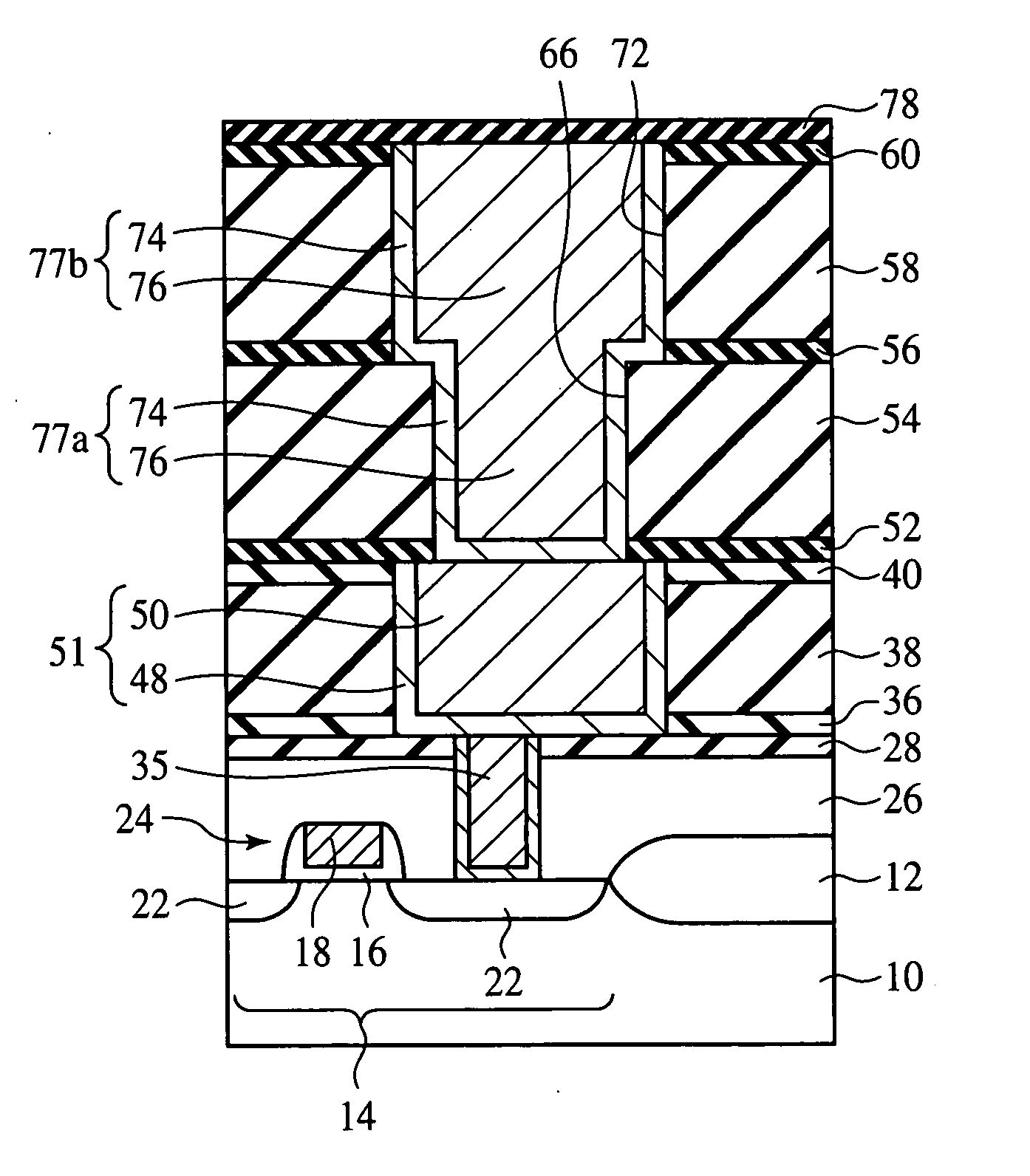
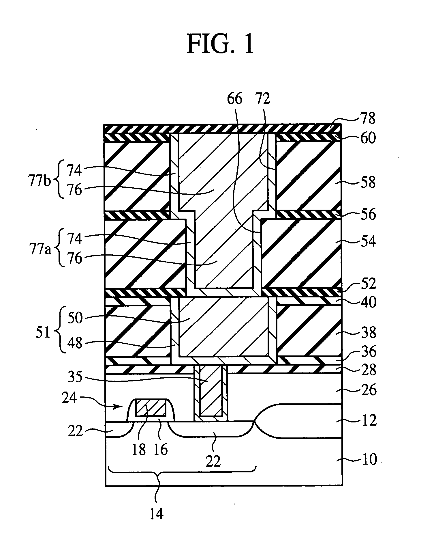
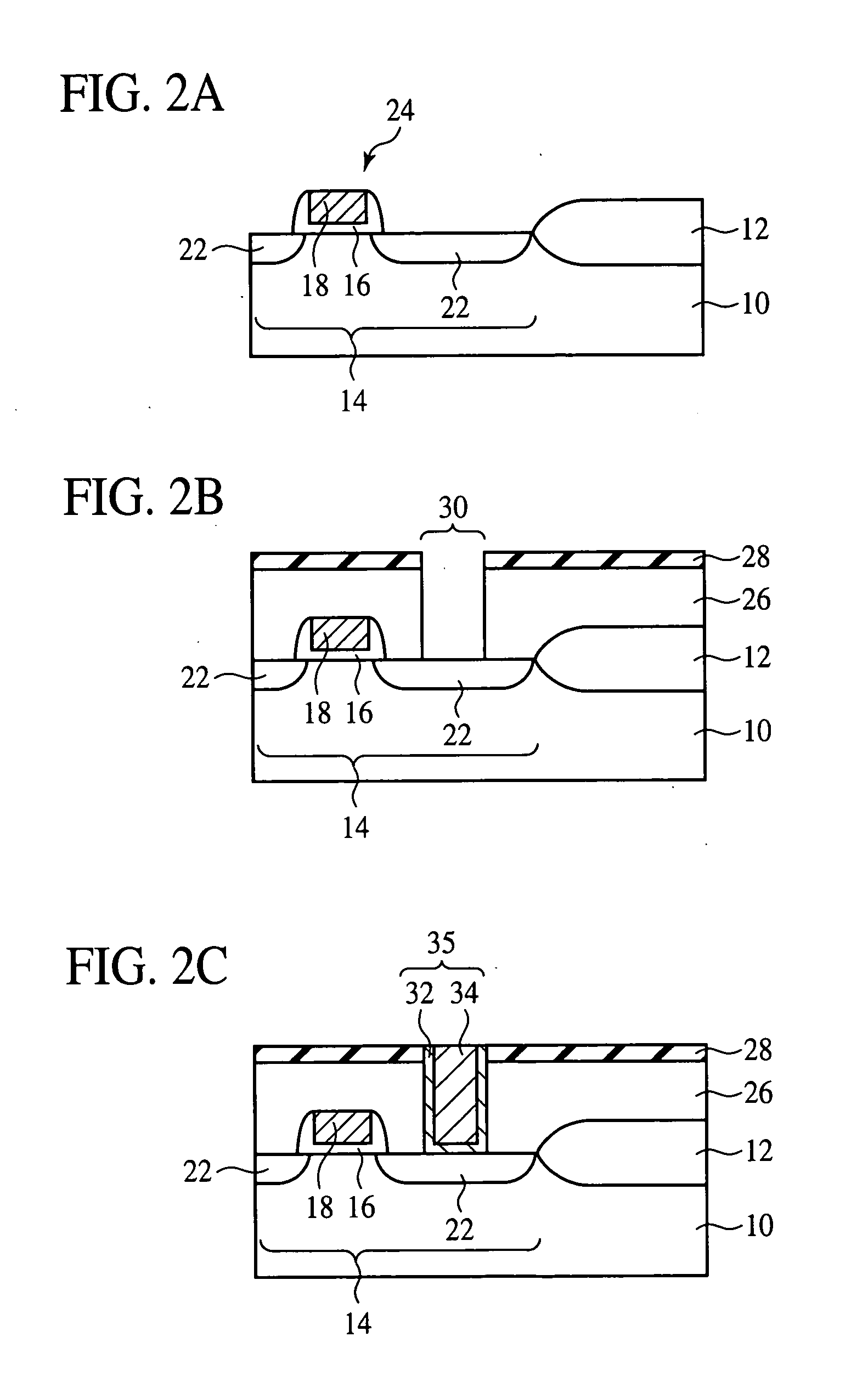
The method for fabricating a semiconductor device comprises the step of forming a first insulating film 38 of a porous material over a substrate 10; the step of forming on the first insulating film 38 a second insulating film 40 containing a silicon compound containing Si—CH3 bonds by 30-90%, and the step of irradiating UV radiation with the second insulating film 40 formed on the first insulating film 38 to cure the first insulating film 38. Thus, UV radiation having the wavelength which eliminates CH3 groups is sufficiently absorbed by the second insulating film, whereby the first insulating film is highly strengthened with priority by the UV cure, and the first insulating film can have the film density increased without having the dielectric constant increased.
Description
CROSS-REFERENCE TO RELATED APPLICATIONS [0001] This application is based upon and claims the benefit of priority from the prior Japanese Patent Application No. 2006-093438, filed on Mar. 30, 2006, the entire contents of which are incorporated herein by reference. BACKGROUND OF THE INVENTION [0002] The present invention relates to a composition for forming an insulating film and a method for fabricating a semiconductor device, more specifically, a method for fabricating a semiconductor device including a porous insulating film, and a composition for forming a porous insulating film. [0003] As the integration and the density of semiconductor integrated circuits are increased, the semiconductor devices are required to have more multi-level structures. On the other hand, with the increasing integration, the interconnection pitch becomes smaller, and the interconnection delay due to increased capacitances between the interconnections is a problem. [0004] An interconnection delay is influ...
Claims
Login to View More Application Information
Patent Timeline
 Patent Type & Authority Applications(United States)
IPC IPC(8): H01L21/4763
CPCC09D183/14C09D183/16H01L21/02126H01L21/022H01L21/02203H01L21/31695H01L21/02222H01L21/02282H01L21/02348H01L21/31633H01L21/02211H01L21/02164H01L21/02216H01L21/31
Inventor OZAKI, SHIROUNAKATA, YOSHIHIROYANO, EI
Owner FUJITSU LTD