RF transceiver switching system

a transceiver switching and transceiver technology, applied in the field of electronic circuits, can solve the problems of large voltage swings at the antenna of these devices, significant current draw, and none of the aforesaid technologies widely used to implement the transmit/receive switch, and achieve the effects of low cost, higher integration level, and robustness

Inactive Publication Date: 2007-10-04
RESONANCE SEMICON CORP
View PDF7 Cites 142 Cited by
  • Summary
  • Abstract
  • Description
  • Claims
  • Application Information

AI Technical Summary

Benefits of technology

[0009] The instant application provides a system and method of creating a transmit / receive switch function using a BiCMOS or CMOS IC process, which allows for a single chip architecture. This includes silicon-based MOS and BJT transistor shunt switches and silicon diode-based shunt switches preferably formed using CMOS or BiCMOS technology. Such shunt switch devices are not required to withstand the voltage swings found at the antenna of the device in FIG. 1. Critical advantages of this solution are that it results in a lower cost, more robust solution with a higher level of integration for RF transceiver front ends.

Problems solved by technology

This means that large voltage swings exist at the antenna of these devices.
PIN diodes have also been used for this application, but they have the drawback that they draw significant current whereas the aforementioned SOS and HEMT technologies do not draw significant current.
Note that none of the aforesaid technologies widely used to implement the transmit / receive switches shown in FIG. 7 are easily integrated with advanced CMOS or BiCMOS IC processes.
Such multi-chip or multilayer laminates can have high manufacturing costs and reliability issues, rendering them undesirable for many applications.
However, all of these approaches create a large voltage stress either between the substrate and the well or between the well and the source and drain junctions.
This can damage or destroy the switch, thereby rendering the transceiver inoperable.
Therefore, the long term reliability of these approaches is questionable.

Method used


Image

  • RF transceiver switching system
  • RF transceiver switching system
  • RF transceiver switching system

Examples


Embodiment Construction

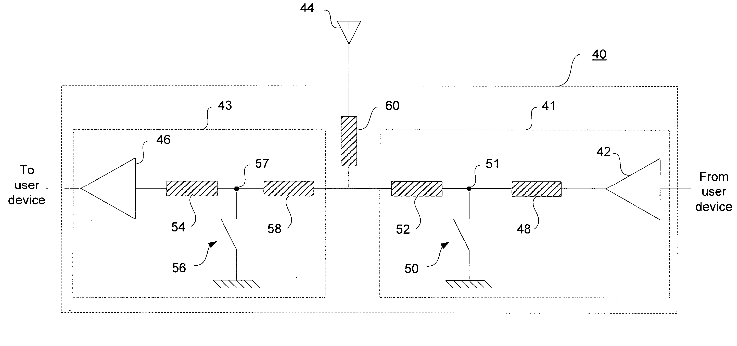
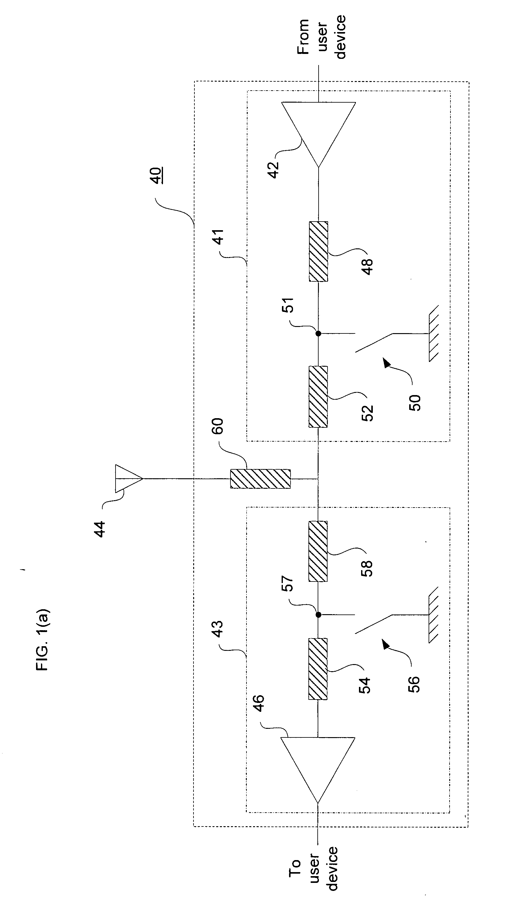
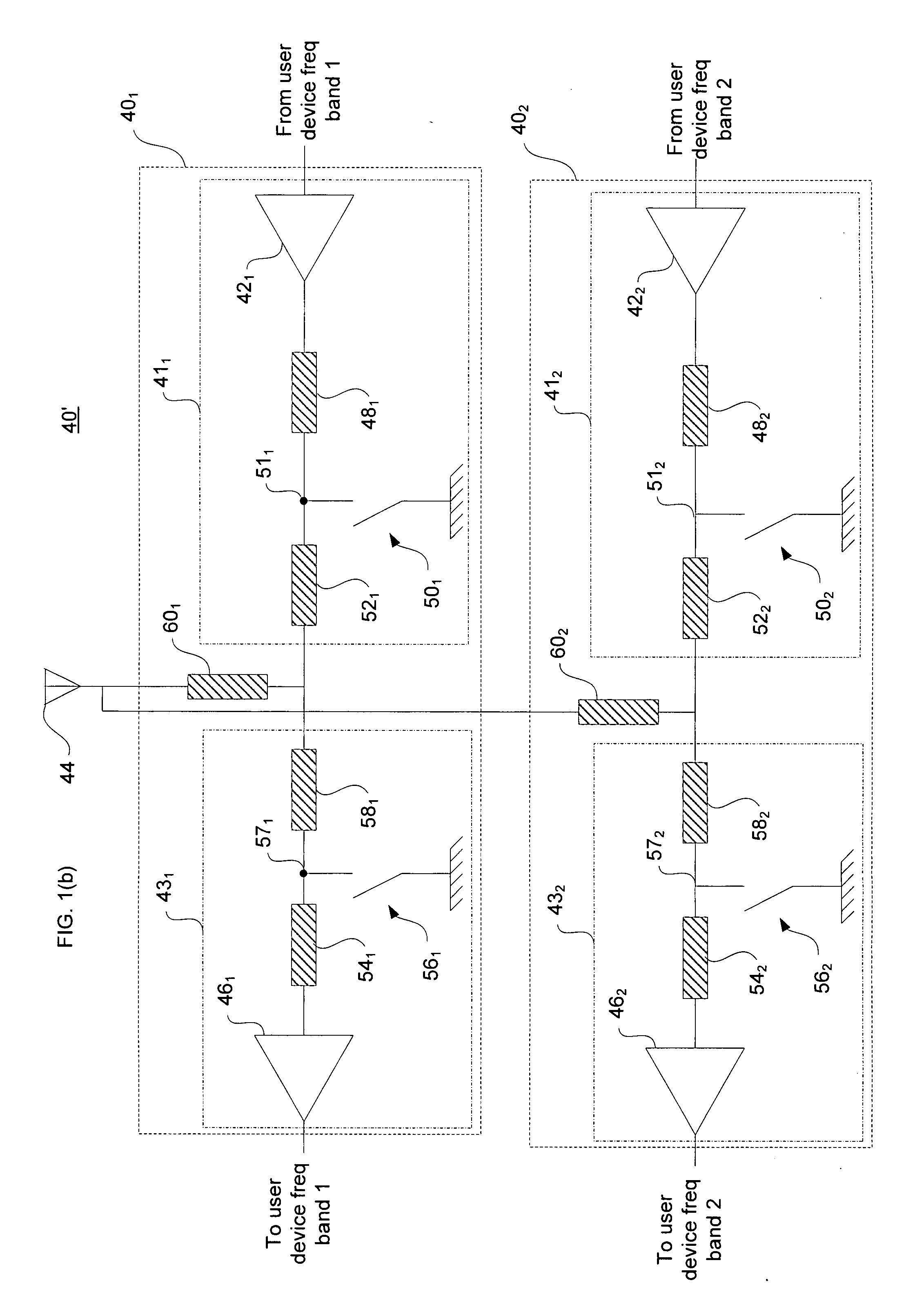
[0024] In describing the preferred embodiments of the invention illustrated in the appended drawings, specific terminology will be used for the sake of clarity. However, the invention is not intended to be limited to the specific terms used, and it is to be understood that each specific term includes all technical equivalents that operate in a similar manner to accomplish a similar purpose.

[0025] The present invention does not involve overall transceiver system architecture design, but rather addresses transceiver switching circuitry that may be employed in different transceiver architectures. A generalized discussion of transceiver architecture design may be found in “Transceiver System Design for Digital Communications,” by Scott R. Bullock, ©1995, ISBN 1-884932-40-0, the entire disclosure of which is hereby expressly incorporated by reference herein.

[0026] One of the critical issues addressed by the present invention involves avoiding high voltage swings that can occur during o...


PUM


Abstract

The present invention relates to transceiver systems and methods which employ shunt switches during transmit and receive operating modes. The shunt switches may be configured with various reactive networks to achieve high or low impedance states at power amplifiers or low noise amplifiers in order to reflect or transmit power along a given path. The shunt switches are designed for protection against excessive voltage swings that would otherwise damage components in the transceiver switching circuit. The switching circuits may be implemented in a single chip architecture, which results in manufacturing efficiencies, lower cost and higher reliability circuits. Single or multi band devices may also be employed.

Description

CROSS-REFERENCE TO RELATED APPLICATIONS [0001] This application claims the benefit of the filing date of U.S. Provisional Patent Application No. 60 / 777,473 filed Feb. 28, 2006 and entitled “A Narrow Band BiCMOS Transmit Receive Switching Scheme for use in Radio Frequency Transceivers,” the entire disclosure of which is hereby incorporated by reference herein.BACKGROUND OF THE INVENTION [0002] The present invention relates to electronic circuits that are radio frequency (“RF”) transceivers; in particular at different times the circuit is required to either transmit RF power to an antenna port or to receive RF power from the antenna port and amplify the signal in a low noise amplifier (“LNA”) on one or more separate frequency bands. [0003] In recent years the use of wireless communications systems has increased significantly. Cellular and cordless telephone systems are ubiquitous. Portable wireless data devices are indispensable to many businesspeople and can be used to send and recei...

Claims


Application Information

Patent Timeline
Patent Type & Authority Applications(United States)
IPC IPC(8): H04B1/44
CPCH04B1/48H04B1/44
Inventor CARLEY, L. RICHARDMETAXAKIS, EMMANOUILSAMELIS, APOSTOLOS
Owner RESONANCE SEMICON CORP
Why Eureka
Try Eureka