
Field effect transistor comprising gold layer, microfluidic device comprising the field effect transistor, and method of detecting analyte having thiol group using the field effect transistor and the microfluidic device

a field effect transistor and gold layer technology, applied in the field of field effect transistors, can solve the problems of deterioration of the sensitivity of the conventional fet for use as a sensor, poor sensitivity of the conventional fet,

Active Publication Date: 2007-10-11
SAMSUNG ELECTRONICS CO LTD
View PDF16 Cites 19 Cited by
  • Summary
  • Abstract
  • Description
  • Claims
  • Application Information

AI Technical Summary

Benefits of technology

[0018]According to an exemplary embodiment of the present invention, there is provided a method of detecting an analyte having a thiol group using the microfluidic device including an inlet and an outlet, each in fluid communication with a microchannel, the microfluidic device including a field effect transistor, the field effect transistor comprising a substrate, a source region and a drain region formed apart from each other on the substrate and doped such that a polarity of the source and drain region is opposite to a polarity of the substrate, a ch...

Problems solved by technology

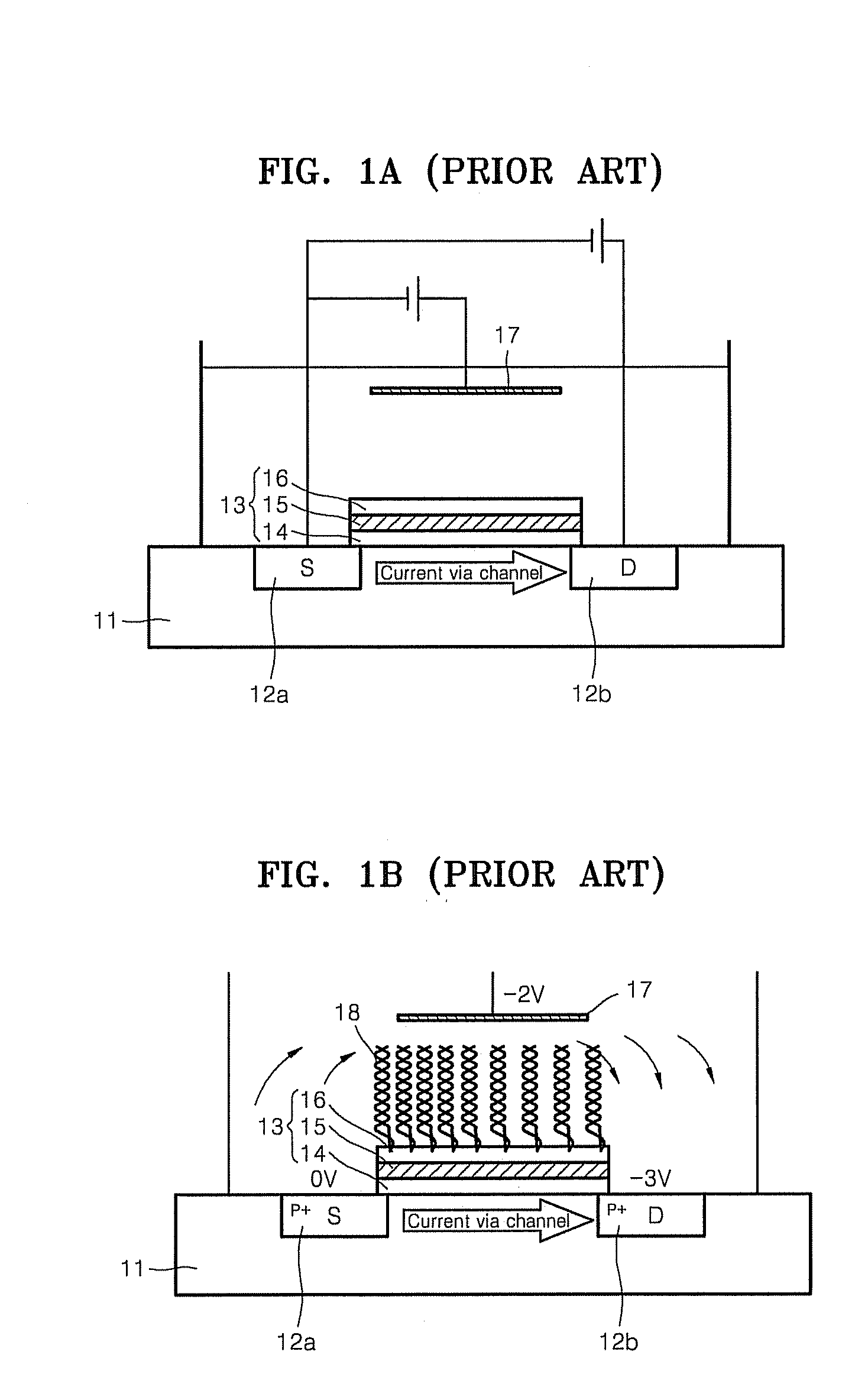
In conventional FETs, the current flowing through the channel of the FET is greatly affected by the ion concentration of an analyte, and sensitivity of the conventional FET is poor.
The reason for the poor sensitivity of the FET is that an increase in ion concentration of the analyte causes masking of molecular charges and subsequent deterioration of the sensitivity of the FET for use as a sensor.
However, in the case of a lab-on-a-chip (“LOC”), the LOC is required to perform a series of processes on the same chip, including measurement, as well as collection, separation, amplification and purification of the sample to be analyzed, and solutions used in these serial processes typically have high ion concentrations.

Method used


Image

  • Field effect transistor comprising gold layer, microfluidic device comprising the field effect transistor, and method of detecting analyte having thiol group using the field effect transistor and the microfluidic device
  • Field effect transistor comprising gold layer, microfluidic device comprising the field effect transistor, and method of detecting analyte having thiol group using the field effect transistor and the microfluidic device
  • Field effect transistor comprising gold layer, microfluidic device comprising the field effect transistor, and method of detecting analyte having thiol group using the field effect transistor and the microfluidic device

Examples


example 1

Production of FET-Based Biosensor

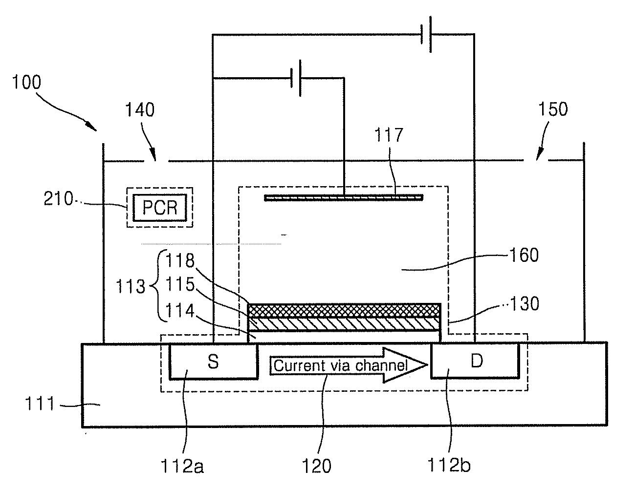
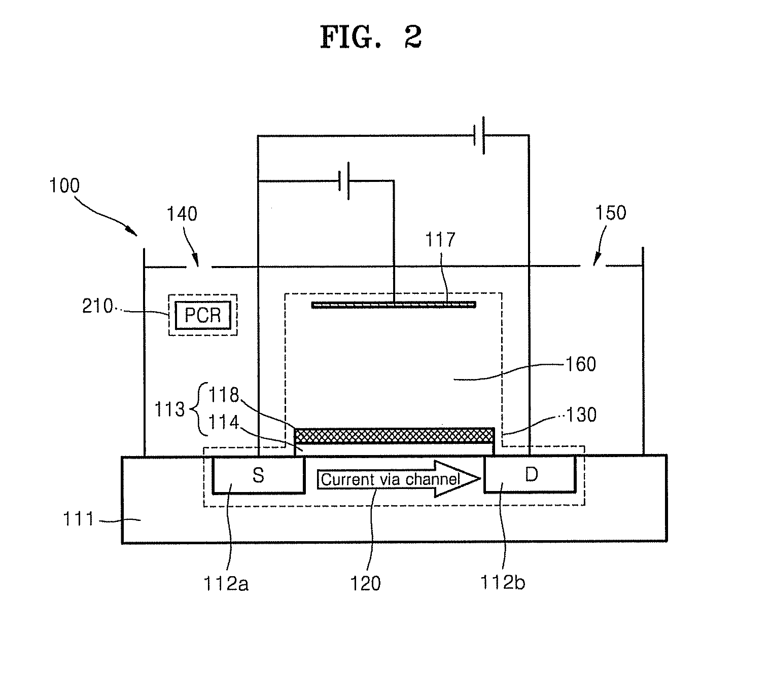
[0060]The FET element used in this example was produced using the facilities of X-FAB Semiconductor Foundries AG in Germany, using the KC10-1.0 μm CMOS manufacturing process of the company. The produced FET element was of NMOS type. The produced FET element had 192 FETs including an identical structure and electrical characteristics, which were arranged in an array (12 FETs×16 rows) on a substrate. CMOS manufacturing processes may vary slightly from company to company, however the process itself is not a factor having a large influence on the characteristics of FET elements. Since the CMOS manufacturing process used by the company is irrelevant to the scope of the present invention, a description thereof will not be provided here. Each of the FET element used in this example has the same structure that of used in Comparative example 1 except that the polysilicon layer 15 and the gate electrode layer 16 has been replaced with a gold layer 118.

[0061]Fi...

example 2

Detection of PCR Product Labeled with Thiol Group, Using FET

[0064]

[0065]DNA amplification was performed by PCR, using the genome of Staphylococcus aureus as the template, and using a forward primer (5′-HS-(CH2)6-TAG CAT ATC AGA AGG CAC ACC C-3′: SEQ ID NO: 1) and a reverse primer (5′-HS-(CH2)6-ATC CAC ATC AGA GAG ACA AC ATT-3′: SEQ ID NO:2). Since the obtained PCR product, including the amplification product as well as the residual primers, included thiol groups, thus being reactive with gold (Au) on the FET element, the PCR product was subjected to purification. The purification was performed in the same manner as in Comparative Example 1. 250 μl of a binding buffer (PB buffer, QIAquick®) and 50 microliter (pi) of the PCR product were mixed, and the resulting mixture was injected into a purification tube of a Qiagene kit, which was then aspirated by a vacuum for 10 to 30 seconds. Next, 750 μl of a washing buffer (PE buffer, QIAquick®) was injected into the purification tube, which ...


PUM


Abstract

A field effect transistor for detecting an analyte having a thiol group includes a substrate, a source region and a drain region formed apart from each other on the substrate, the source region and the drain region being doped such that a polarity of the source and drain region is opposite to a polarity of the substrate, a channel region disposed between the source region and the drain region, an insulating layer formed of an electrically insulating material and disposed on the channel region, a gold layer disposed on the insulating layer and a reference electrode disposed apart from the gold layer.

Description

[0001]This application claims priority to Korean Patent Application No. 10-2006-0032413, filed on Apr. 10, 2006, and all the benefits accruing therefrom under 35 U.S.C. §119, the contents of which in its entirety are herein incorporated by reference.BACKGROUND OF THE INVENTION[0002]1. Field of the Invention[0003]The present invention relates to a field effect transistor (“FET”) having a gold layer, a microfluidic device including the FET and a method of detecting an analyte having a thiol group using the FET and the microfluidic device.[0004]2. Description of the Related Art[0005]A class of sensors for detecting biomolecules with electrical signals includes transistor-based biosensors having a structure including a transistor. These transistor-based biosensors are produced by applying the techniques of semiconductor processes, and are advantageous in terms of rapid conversion of electrical signals, easy integration of microelectromechanical systems (“MEMS”) with integrated circuits ...

Claims


Application Information

Patent Timeline
IPC IPC(8): H01L31/00
CPCG01N27/4145H01L29/78B42D1/08B42F5/00B42D1/009
Inventor SHIM, JEO-YOUNGYOO, KYU-TAELEE, KYU-SANGCHUNG, WON-SEOKCHO, YEON-JAYOO, CHANG-EUN
Owner SAMSUNG ELECTRONICS CO LTD
Learn More