Plating apparatus and plating method

a technology of plating apparatus and plating method, which is applied in the direction of liquid/fluent solid measurement, fluid pressure measurement, peptides, etc., can solve the problem of increasing the difficulty of forming a plated film having a sufficient in-plating uniform thickness of a plated film over an entire surface, increasing the variation of the thickness of a plated film formed on a surface or a substrate, and increasing the difficulty of forming a plated film having a sufficien

Inactive Publication Date: 2007-10-11
EBARA CORP
View PDF9 Cites 71 Cited by
  • Summary
  • Abstract
  • Description
  • Claims
  • Application Information

AI Technical Summary

Benefits of technology

[0107] The electric field can be made more uniform over an entire surface of a substrate also by adjusting the overall electric resistance between upper and lower surfaces of a porous structure with its interior filled with an electrolytic solution to not less than 0.02 time the sheet resistance of a surface conductive layer of the substrate. Thus, in the case where the electrolytic processing is plating, the in-plane uniformity of a thickness of a plated film formed on the surface of the substrate can be enhanced.

Problems solved by technology

As a seed layer becomes thinner and the sheet resistance of a surface (surface to be plated) of a substrate becomes higher with the progress toward seed layer-less substrates, it becomes more and more difficult to form a plated film having a uniform thickness over an entire surface of a substrate having fine interconnect recesses formed in the surface while securely filling the interconnect recesses with the metal (interconnect material) without forming voids in the embedded metal.
It is considered, however, that variation in the thickness of a plated film formed on a surface or a substrate becomes increasingly larger in the next 45 nm-node generation and the following 32 nm-node generation and the formation of a plated film having a sufficient in-plating uniformity of plated film thickness becomes increasingly difficult.
Further, it is generally difficult to produce such a plated film as not to impose a burden on a CMP processing while preventing deterioration of the quality of the plated film and scratches in a surface of the plated film.
In this sense, the existing semiconductor manufacturing process is not perfect.

Method used


Image

  • Plating apparatus and plating method
  • Plating apparatus and plating method
  • Plating apparatus and plating method

Examples


Embodiment Construction

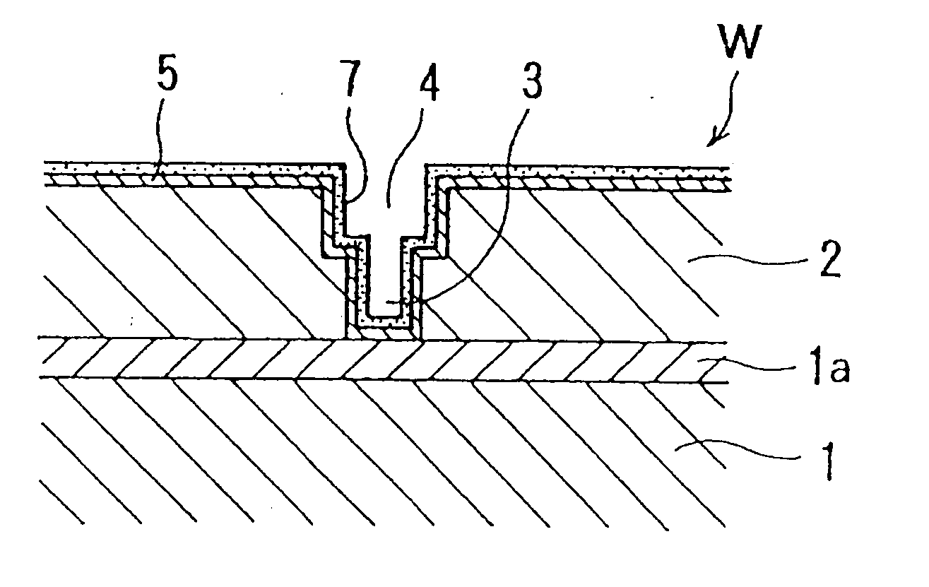
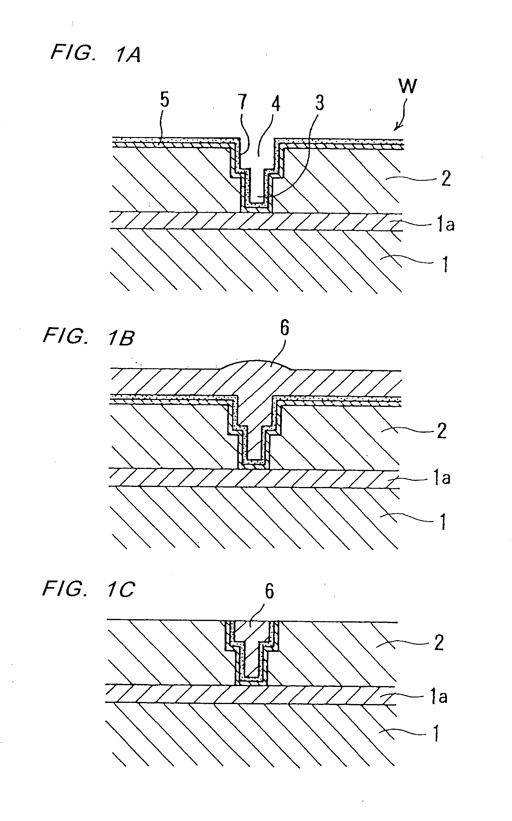
[0153] Preferred embodiments of the present invention will now be described in detail with reference to the drawings. The following embodiments relate to the application of the present invention useful for forming interconnects of copper by embedding copper in fine interconnect recesses formed in a surface of the substrate.

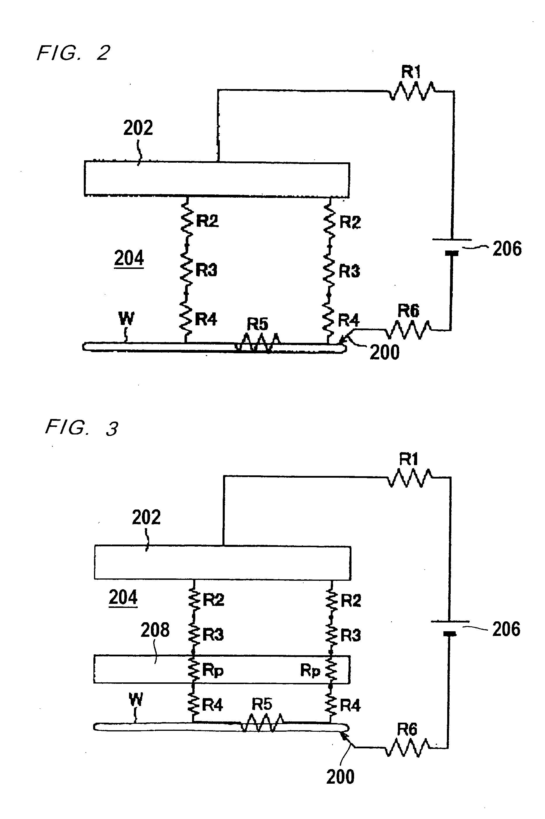
[0154]FIG. 5 is an overall layout showing a substrate processing apparatus incorporating a plating apparatus according to an embodiment of the present invention. As shown in FIG. 5, this substrate processing apparatus has a facility which houses therein two loading / unloading units 10 for housing a plurality of substrates W therein, two plating apparatuses 12 for performing plating process, a transfer robot 14 for transferring substrates W between the loading / unloading units 10 and the plating apparatuses 12, and plating solution supply equipment 18 having a plating solution tank 16.

[0155] The plating apparatus 12, as shown in FIG. 6, is provided with a substrate...


PUM

PropertyMeasurementUnit
diameteraaaaaaaaaa
surface roughnessaaaaaaaaaa
pressure lossaaaaaaaaaa

Abstract

A plating apparatus can form a plated film having a more uniform thickness over an entire surface of a substrate and can securely fill interconnect recesses with the metal without forming voids in the embedded metal even when the substrate has a high sheet resistance in the surface. The plating apparatus includes a substrate holder for holding a substrate, a cathode portion including a cathode for contact with the substrate held by the substrate holder to feed electricity to the substrate, and an anode, partly or wholly having a high resistance, disposed opposite a surface of the substrate held by the substrate holder, wherein plating of the surface of the substrate is carried out while filling between the anode and the substrate held by the substrate holder with a plating solution.

Description

BACKGROUND OF THE INVENTION [0001] 1. Field of the Invention [0002] The present invention relates to a plating apparatus and a plating method, and more particularly to a plating apparatus and a plating method used for filling fine interconnect recesses (circuit pattern) formed in a substrate, such as a semiconductor substrate, with metal (interconnect material) such as copper so as to form interconnects. [0003] The present invention also relates to an electrolytic processing apparatus and an electrolytic processing method used for electrolytic processing such as electroplating. [0004] 2. Description of the Related Art [0005] In recent years, instead of using aluminum or aluminum alloys as a material for forming interconnect circuits on a semiconductor substrate, there is an eminent movement towards using copper that has a low electric resistivity and high electromigration resistance. Such copper interconnects are generally formed by filling copper into fine interconnect recesses for...

Claims


Application Information

Patent Timeline
Patent Type & Authority Applications(United States)
IPC IPC(8): C25D3/00B05C9/08B32B15/04
CPCH01L21/2885H01L21/7684C25D17/001C25D7/123H01L21/76877
Inventor KURASHINA, KEIICHINAKADA, TSUTOMUKAWAKAMI, TAKASHIYAMAMOTO, SATORUHAYABUSA, KEISUKE
Owner EBARA CORP
Why Eureka
Try Eureka