
Architecture and method for providing integrated circuits

Inactive Publication Date: 2007-10-11
QUADRIC
View PDF0 Cites 0 Cited by
  • Summary
  • Abstract
  • Description
  • Claims
  • Application Information

AI Technical Summary

Benefits of technology

[0013] The present invention completes the transformation to soft design, and thus represents a third technological solution to implement custom Integrated Circuits. In accordance with the principles of the invention a single chip processor, specially architected in accordance with the principles of the invention, is provided that is customizable to provide customer specified logic functions and interconnects. The architecture runs software code in parallel, and further in accordance with the principles of the invention, performs all the customized logic and interconnect functions. The specially-architected processor is even easier to customize, but still outperforms and uses less power, than an FPGA while remaining much less expensive to produce. Compared to an ASIC, it is orders of magnitude less costly to customize, while approaching the performance level of an ASIC.

Problems solved by technology

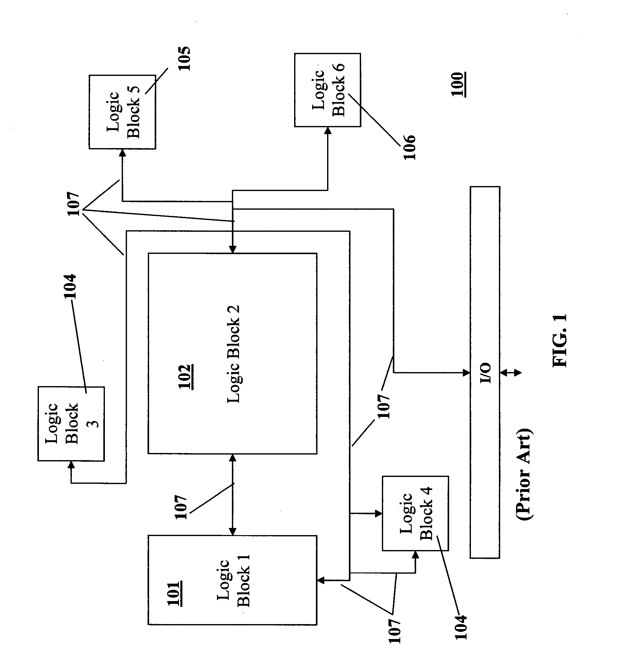
Though custom lCs have existed since the dawn of the semiconductor industry, the effects of Moore's law have increased the complexity of ICs to such an extent that the nature of the design has changed.
The pros and cons consist of tradeoffs between development time and cost, recurring parts costs, and performance.
ASIC technology has high performance and low recurring cost, but can cost tens of millions of dollars to design at 180 nm and below.
The technology is hard-wired, meaning that it cannot be changed once it is manufactured.
The schedules are long, especially when re-spins are necessary, and the risks are enormous.
The cost to develop an FPGA is much less than ASIC, but the chips are much larger than an equivalent ASIC, so recurring costs are far higher, e.g., $2500 per device at the high end.
Further, performance is much lower and power consumption is higher than ASIC.
System designers must, then choose the right technology based on requirements, but there is always a tradeoff between development and recurring costs and levels of performance.
The design costs, and thus risks, associated with ASICs and FPGAs are driven by the staffing necessary to implement the hardware design.
FPGAs mitigate the risk by allowing changes in the field, but tradeoff this advantage with decreased performance and increased parts costs.

Method used


Image

  • Architecture and method for providing integrated circuits
  • Architecture and method for providing integrated circuits
  • Architecture and method for providing integrated circuits

Examples


first embodiment

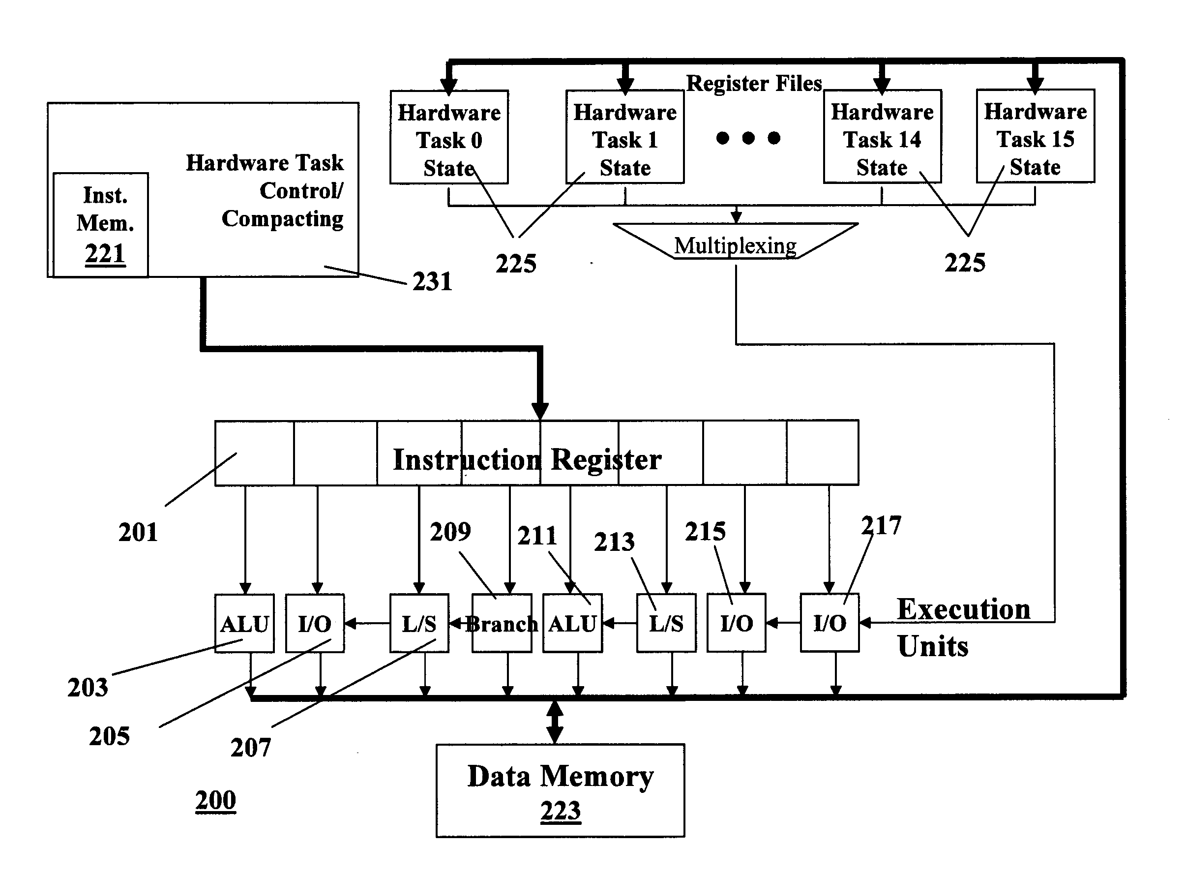
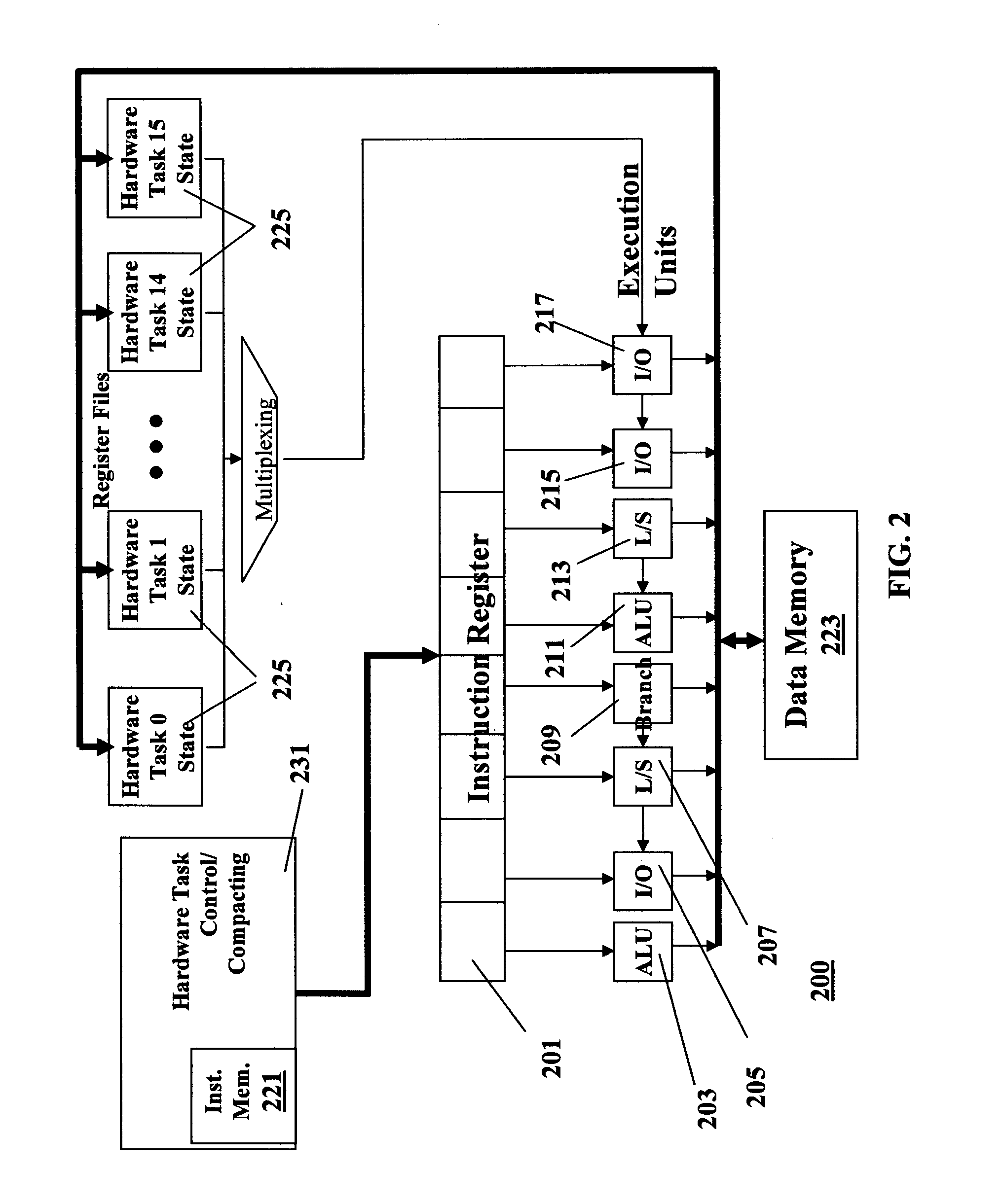
[0034] A first embodiment architecture in accordance with the principles of the invention is shown in FIG. 2. The architecture of FIG. 2 is a meta-processor 200 that allows concurrent execution of many tasks. It is based on a Very Long Instruction Word (VLIW) architecture, which has natural concurrency as part of the architecture. Users of the present invention design the hardware functions with software tools, dramatically reducing development costs.

[0035] The architecture of the present invention is a VLIW meta-processor that is a super ‘bit-bang’ machine, i.e., a processor that toggles the I / O of a chip using software, rather than hardware. Logic is implemented in software, running the algorithms that today's ASICs and FPGAs perform in hardware. Interconnect is implemented through memory mailboxes between programs. Both are described in more detail below.

[0036] VLIW processors differ from typical processors, e.g. the x86 series, in the length of the instruction word. Typical pro...

second embodiment

[0079]FIG. 14 shows a second embodiment architecture in accordance with the principles of the invention, meant to perform the functions in FIG. 13. A difference in architecture is the addition of instruction memory 221 on-chip, outside of the task control / compacting unit 231. This is because the hardware tasks will be much more complicated, especially when running processor code. Thus the code for each hardware task is located in the instruction memory 221 while the task control / compacting unit 231 contains cache instead of simple instruction memory.

[0080] The instruction length is 512 bits, made up of sixteen 32-bit instructions as shown in FIG. 15. It is substantially the same as the logic-only embodiment, with 32-bit-wide instruction words instead of 16.

[0081] Execution units 203, 1401, 205, 207, 209, 211, 213, 215, 217 are substantially identical to the logic-only version, except they are all 32-bit wide instead of 16 or 12.

[0082] The hardware task code is generated in an iden...


PUM


Abstract

A customizable integrated circuit is programmed to provide both hardware task functions and interconnects. A plurality of execution units is executable concurrently to emulate hardware tasks. A plurality of programmable locations provides logical interconnect between the executable programs.

Description

RELATED APPLICATIONS [0001] This application claims the benefit of and priority based upon U.S. provisional application for patent 60 / 790,637 filed on Apr. 10, 2006.FIELD OF THE INVENTION [0002] The invention pertains to integrated circuit design, in general, and to a system and method of providing customized integrated circuits, in particular. BACKGROUND OF THE INVENTION [0003] There is a demand for customized Integrated Circuits (“ICs”). Customization allows companies to differentiate themselves from the competition by placing specialized, user-specific functions on the IC. Though custom lCs have existed since the dawn of the semiconductor industry, the effects of Moore's law have increased the complexity of ICs to such an extent that the nature of the design has changed. Those changes will continue in the future, creating a need to improve design productivity dramatically. [0004] Designing a custom chip is an exercise in defining two items: (a) logic, which takes input signals, p...

Claims


Application Information

Patent Timeline
IPC IPC(8): G06F17/50H03K19/00
CPCG06F17/5054G06F30/34
Inventor SHORT, PAUL
Owner QUADRIC
Learn More