Exposure Apparatus, Exposure Method and Device Manufacturing Method, and Surface Shape Detection Unit

a technology of surface shape detection and exposure apparatus, which is applied in the direction of instruments, optics, transmission, etc., to achieve the effect of good productivity and good productivity

Inactive Publication Date: 2007-10-25
NIKON CORP
View PDF23 Cites 71 Cited by
  • Summary
  • Abstract
  • Description
  • Claims
  • Application Information

AI Technical Summary

Benefits of technology

[0014] With this apparatus, the information of a surface shape of a substantially entire area of the surface subject to exposure of the object can be obtained in a short period of time.
[0015] Further, in a lithography process, by transferring a device pattern onto an object using the exposure apparatus of the present invention, microdevices of higher-integration can be manufactured with good productivity. Accordingly, it can also be said from another aspect that the present invention is a device manufacturing method that includes a lithography process using the exposure apparatus of the present invention. Likewise, in a lithography process, by transferring a device pattern onto an object using the exposure method of the present invention, microdevices of higher-integration can be manufactured with good productivity. Accordingly, it can also be said further from another aspect that the present invention is a device manufacturing method that includes a lithography process using the exposure method of the present invention.

Problems solved by technology

According to the larger diameter of the lens, a distance between the lens and the substrate (the so-called working distance) becomes smaller, which makes it difficult as a consequence to arrange the multipoint AF system.

Method used


Image

  • Exposure Apparatus, Exposure Method and Device Manufacturing Method, and Surface Shape Detection Unit
  • Exposure Apparatus, Exposure Method and Device Manufacturing Method, and Surface Shape Detection Unit
  • Exposure Apparatus, Exposure Method and Device Manufacturing Method, and Surface Shape Detection Unit

Examples


Embodiment Construction

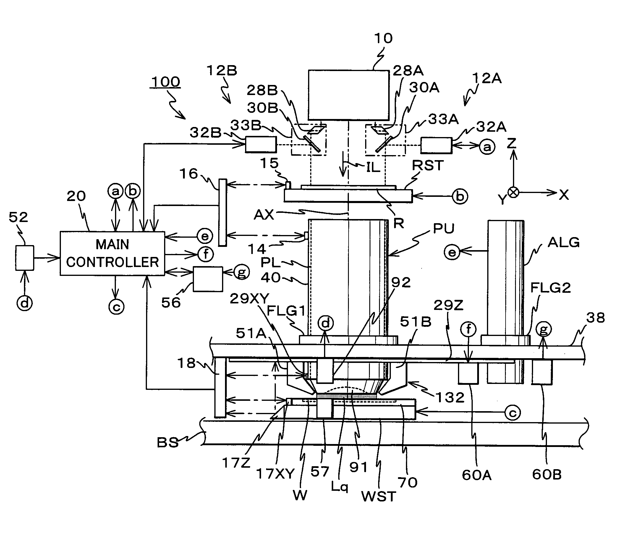
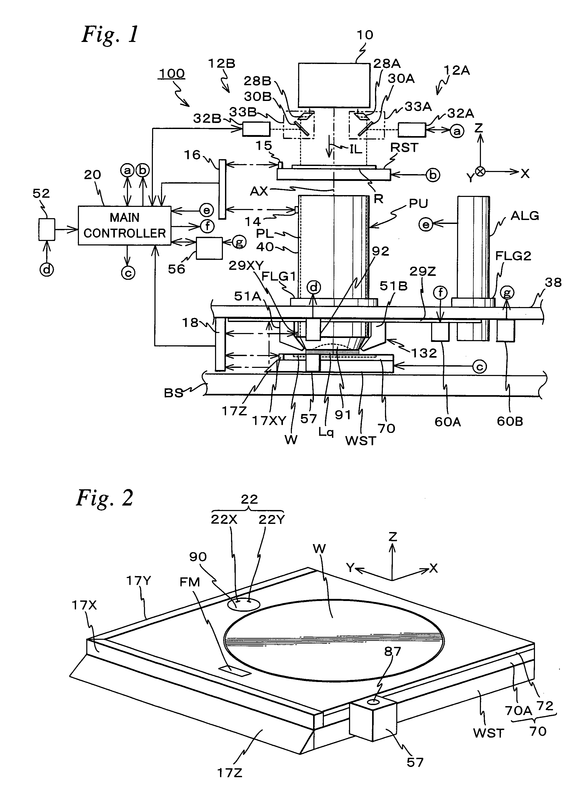
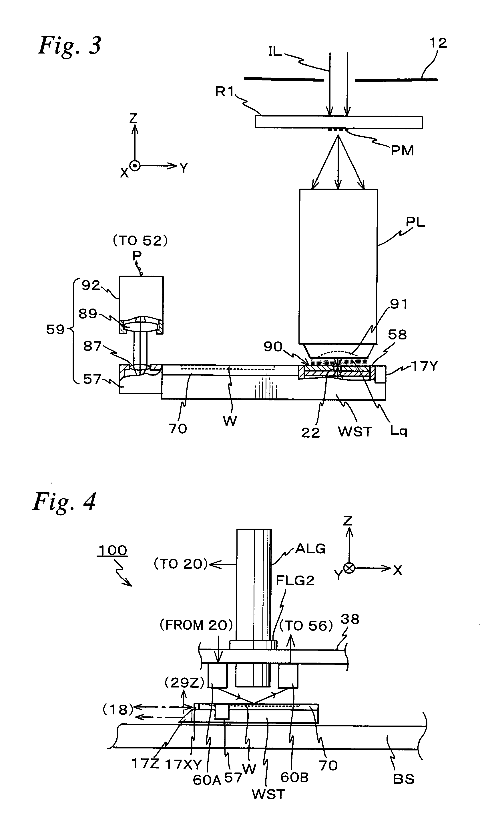
[0036] An embodiment of the present invention will be described based on FIG. 1 to FIG. 11B. FIG. 1 shows the schematic configuration of an exposure apparatus 100 related to an embodiment of the present invention. Exposure apparatus 100 is a projection exposure apparatus by the step-and-scan method (a scanning stepper (also called as a scanner)).

[0037] Exposure apparatus 100 is equipped with an illumination system 10 that includes a light source and illumination optical system (such as a movable reticle blind to be described later) and an illuminates a reticle R with an illumination light (an exposure light) IL as an energy beam, a reticle stage RST holding a reticle R, a projection unit PU, a wafer stage WST where a wafer W is mounted, a body (a part of which is shown in FIG. 1) where reticle stage RST, projection unit PU and the like are mounted, a control system having overall control over the entire apparatus, and the like.

[0038] Illumination system 10 is, for example as discl...


PUM

PropertyMeasurementUnit
wavelengthaaaaaaaaaa
Refractive indexaaaaaaaaaa
wavelengthaaaaaaaaaa

Abstract

In subroutine 201 and step 205, a best image-forming plane of a projection optical system and an offset component of a multipoint AF system are detected as calibration information. During measurement of a wafer alignment mark by an alignment system in step 215, the multipoint AF system detects information related to a surface shape of a surface subject to exposure of a wafer (Z map). In step 219, a Z position order profile regarding position order (Z, θx, θy) related to autofocus leveling control is made, along with an XY position order profile of a wafer stage during scanning exposure, and in step 221, scanning exposure is performed while performing open control based on the position order.

Description

TECHNICAL FIELD [0001] The present invention relates to exposure apparatuses, exposure methods, device manufacturing methods, and surface shape detection units, and more particularly to an exposure apparatus and an exposure method in which on object is exposed via a projection optical system, a device manufacturing method that uses the exposure apparatus or the exposure method, and a surface shape detection unit that detects information related to a surface shape of a surface subject to exposure of the object. BACKGROUND ART [0002] Conventionally, in a lithographic process for manufacturing electronic devices such as semiconductor devices (integrated circuits) and liquid-crystal display devices, a projection exposure apparatus that transfers an image of a pattern on a mask or reticle (hereinafter generally referred to as a ‘reticle’) onto each shot area on a photosensitive substrate such as a wafer coated with resist (photosensitive agent) or on a glass plate (hereinafter referred t...

Claims


Application Information

Patent Timeline
Patent Type & Authority Applications(United States)
IPC IPC(8): G01B11/30G03F7/20G03F9/00H01L21/027
CPCG03F9/7003H04B7/155G03F9/7019G03F9/7011
Inventor MAGOME, NOBUTAKAMIZUTANI, HIDEOHIDAKA, YASUHIRO
Owner NIKON CORP
Why Eureka
Try Eureka