Pattern decomposition and optical proximity correction method for double exposure when forming photomasks

Active Publication Date: 2007-10-25
SK HYNIX INC
View PDF3 Cites 33 Cited by
  • Summary
  • Abstract
  • Description
  • Claims
  • Application Information

AI Technical Summary

Benefits of technology

[0006]Embodiments of the present invention are directed to a method of optimizing pattern decomposition and optical proximity correction for double exposure whe

Problems solved by technology

As the patterns become finer such that the size of the patterns approaches the limit of resolution, the

Method used


Image

  • Pattern decomposition and optical proximity correction method for double exposure when forming photomasks
  • Pattern decomposition and optical proximity correction method for double exposure when forming photomasks
  • Pattern decomposition and optical proximity correction method for double exposure when forming photomasks

Examples


Embodiment Construction

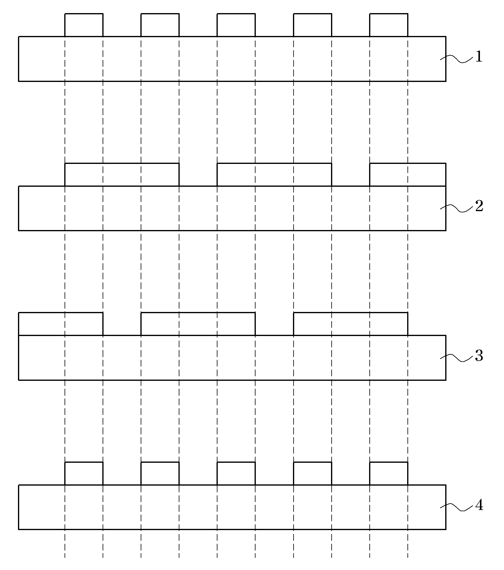
[0025]In a typical double exposure method, an exposing step is repeated twice or more through photomasks, followed by repeating an etching step twice or more corresponding to the respective exposing steps. FIG. 1 is a cross-sectional view of a pattern in each exposing step of a typical double exposure method.

[0026]A first photomask 2 and a second photomask 3 are prepared to form desired patterns on a wafer, that is, target patterns 1, using a double exposure method.

[0027]Primary exposing and etching are sequentially performed using the first photomask 2. Secondary exposing and etching are sequentially performed using the second photomask 3, thereby forming patterns such as the target patterns 1 on the wafer 4.

[0028]The most important double exposure considerations are pattern decomposition to separate the target patterns formed by the respective exposing steps, and optical proximity correction on each of the separated patterns. The optical proximity correction is performed on the ov...


PUM


Abstract

A pattern decomposition and optical proximity correction method for double exposure comprises defining second exposure patterns by performing a logical operation on target patterns and first exposure patterns, comparing the first and second exposure patterns with the target patterns by performing a logical operation on the first and second exposure patterns, performing optical proximity correction on the first exposure patterns to form fourth exposure patterns, performing the optical proximity correction on the second exposure patterns to form fifth exposure patterns, and comparing the fourth and fifth exposure patterns with the target patterns by performing a logical operation on the fourth and fifth exposure patterns.

Description

CROSS-REFERENCE TO RELATED APPLICATION[0001]The present application claims priority to Korean patent application No. 10-2006-0036399, filed on Apr. 21, 2006, which is incorporated herein by reference in its entirety.BACKGROUND OF THE INVENTION[0002]The present invention relates to a method for manufacturing a semiconductor device. More particularly, the present invention relates to a method of optimizing pattern decomposition and optical proximity correction for double exposure when fabricating photomasks.[0003]Due to an increase in the integration degree of a semiconductor device, there is a requirement to form finer patterns through a photolithography process. The photolithography process is used to form circuit patterns on a semiconductor wafer, and generally comprises photoresist coating, exposure, development, and the like. A higher resolution, an optimal depth of focus (DOF), etc. are required to form finer patterns using the photolithography process.[0004]As the patterns beco...

Claims


Application Information

Patent Timeline
IPC IPC(8): G06F17/50G03F1/00G03C5/00
CPCG03F1/36G03F1/144G03F1/70G03F7/70466
Inventor CHOI, JAE SEUNG
Owner SK HYNIX INC
Why Eureka
Try Eureka