Structure and fabrication of self-aligned high-performance organic fets

a technology of organic transistors and structures, applied in the field of organic transistors, can solve the problems of significantly different actual mechanics giving rise to charge carriers in organic semiconductors, significantly different organic transistors, and significantly different inorganic transistors, and achieve the effects of low cost, low channel length devices, and high volum

Inactive Publication Date: 2007-11-01
TAP DEV LLC
View PDF6 Cites 45 Cited by
  • Summary
  • Abstract
  • Description
  • Claims
  • Application Information

AI Technical Summary

Benefits of technology

[0014] According to the present invention, a structure and method of fabrication is disclosed that can produce low channel length devices in high volume and at low cost. The structure includes successively deposited patterned layers of a first conductor layer acting as a source terminal, a first dielectric layer, a second conductor layer acting as a drain terminal, a semiconductor layer, a second dielectric layer, and a third conductor layer acting as the gate terminal. In this structure, the transistor is formed on the edge of the first dielectric between the first conductor layer and the second conductor layer.
[0015] The second conductor layer is deposited on the raised surfaces formed by the dielectric such that the ink does not flow into the trough between the dielectric raised surfaces. In an embodiment of the invention, this is accomplished by coating a flat or rotary print plate with a conductive ink, and applying the appropriate pressure to deposit the materials only on the raised surfaces of the dielectric. In this manner, the second metal is automatically aligned to the layer beneath it. Due to this self-alignment and the short channel formed by the thickness of the dielectric material, a high-performance FET is produced without the requirement of high-resolution lithography equipment.

Problems solved by technology

However, the actual mechanics giving rise to charge carriers in organic semiconductors are substantially different from inorganic semiconductors.
Though organic transistors have much lower performance than inorganic transistors, the materials and processing techniques to produce organic transistors cost significantly less those used to produce inorganic transistors.
Therefore, organic transistor technology has application where low cost is desired and low performance is acceptable.
Low cost printing techniques are generally limited to a minimum range of 25μ.
Printing at resolutions finer than this is generally not possible.
The advantages of the short channel length that can potentially be obtained through vertical transistors is consequently lost.
However, several issues make this fabrication method impractical.
A serious problem with this method is that the metal 408 layer smears when pressing the impression die through the layers, thereby shorting second conductor 408 and first conductor 404.
Another problem with this method is that the die impression forms a point at the bottom of the device, which is very difficult to deposit layers of controlled thickness in this region.
One further problem with this method is that pressure controls the impression die depth of penetration.
If the impression die pressure is too heavy, the impression die will penetrate substrate 402, adversely affecting the performance of the transistors.

Method used


Image

  • Structure and fabrication of self-aligned high-performance organic fets
  • Structure and fabrication of self-aligned high-performance organic fets
  • Structure and fabrication of self-aligned high-performance organic fets

Examples


Embodiment Construction

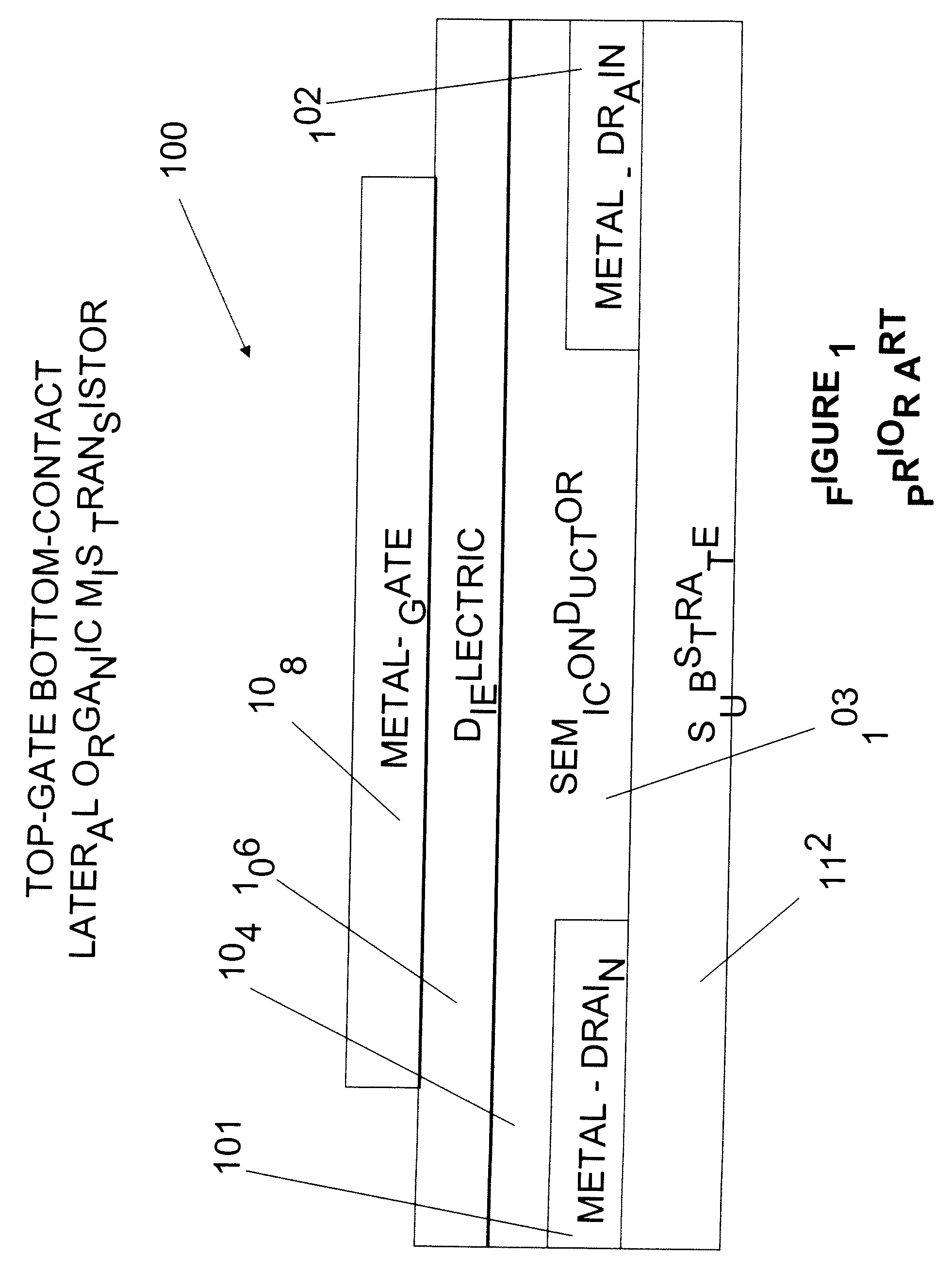
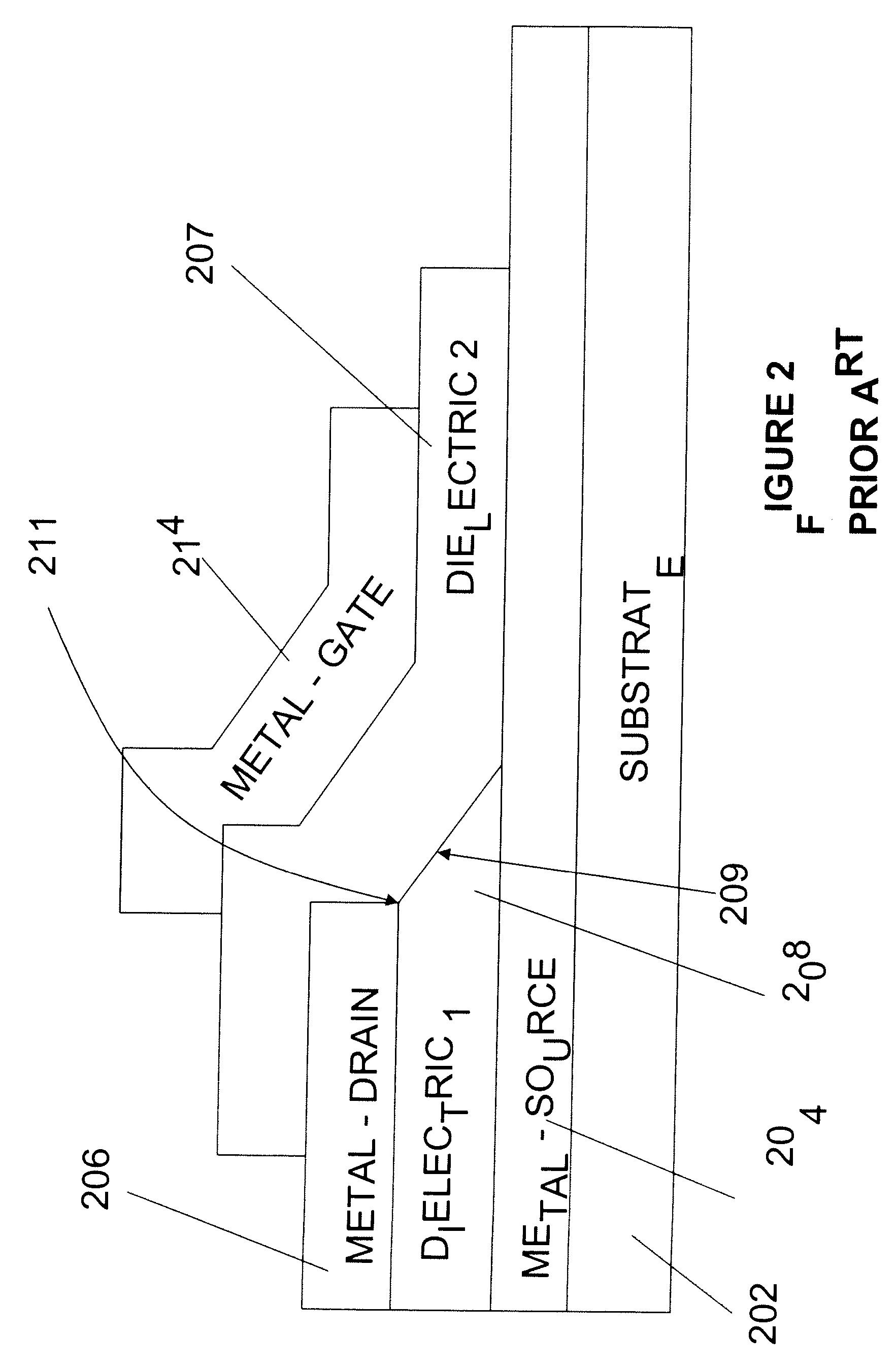
[0025] Referring now to FIG. 5, one embodiment of this invention is illustrated. The structure is formed by depositing successive patterned layers of a conductor metal—source 502, a first insulator dielectric 504, a conductor metal-drain 506, a semiconductor 508, a second insulator dielectric 510, a conductor metal-drain 512 and a conductor metal-gate 514 on substrate 550.

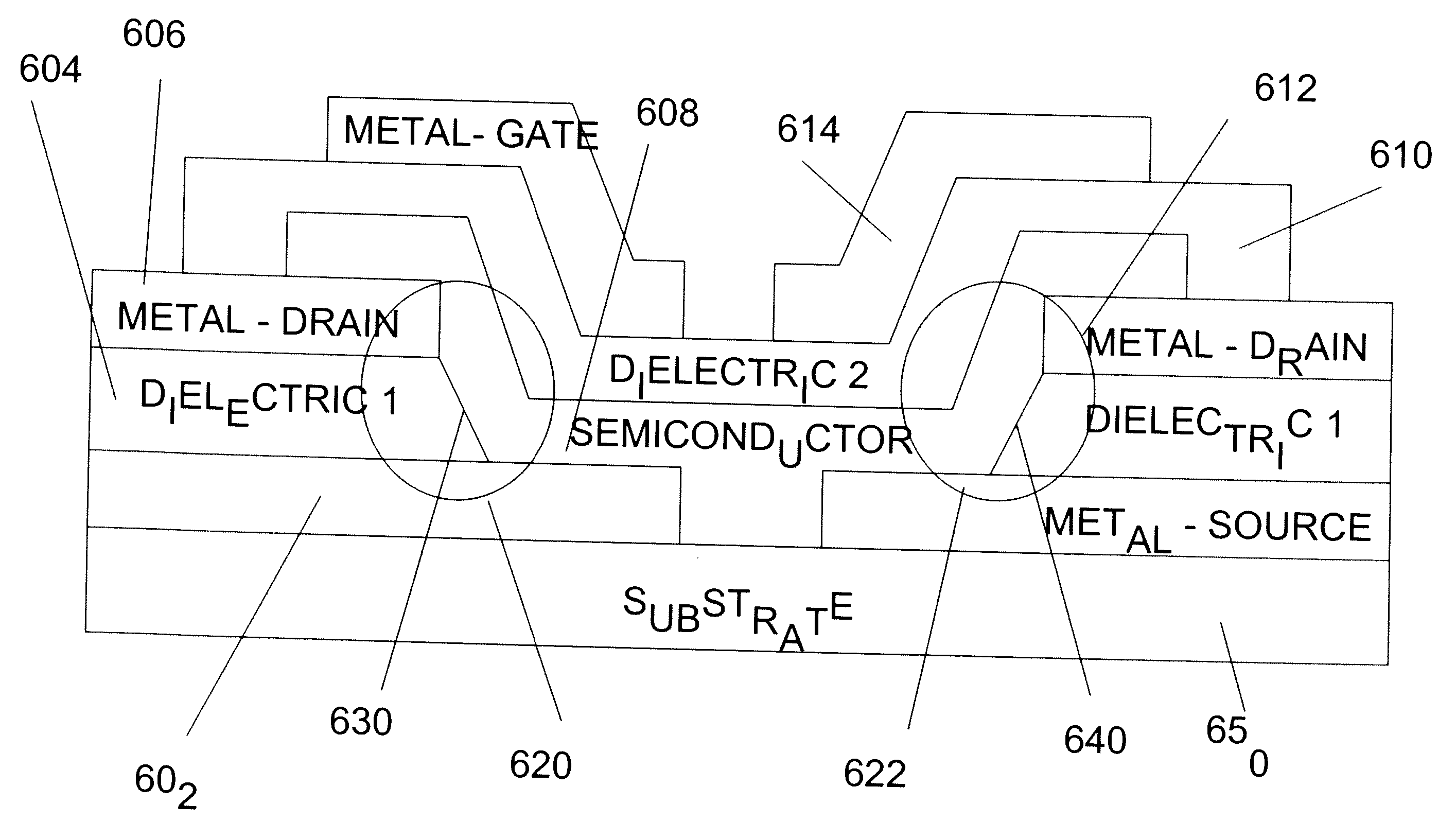
[0026] Referring to FIG. 5, region 520 signifies a transistor formed by this structure. The source of this device is formed by metal source 502, and the drain is formed by metal-drain 506. The vertical space between metal-drain 506 and metal-source 502 forms the channel region 530 of the device in region 520. The channel region 530 is overlapped by successive layers of a semiconductor 508, dielectric 2510, and metal gate 514. The gate terminal of the transistor in region 520 is metal-gate 514.

[0027] Referring to FIG. 5, region 522 signifies a second transistor formed by the same structure. The gap 540 is the chan...


PUM

PropertyMeasurementUnit
thicknessesaaaaaaaaaa
dielectric thicknessaaaaaaaaaa
thickaaaaaaaaaa

Abstract

A low channel length organic field-effect transistor can be produced in high volume and at low cost. The transistor structure includes successively deposited patterned layers of a first conductor layer acting as a source terminal, a first dielectric layer, a second conductor layer acting as a drain terminal, a semiconductor layer, a second dielectric layer, and a third conductor layer acting as the gate terminal. In this structure, the transistor is formed on the edge of the first dielectric between the first conductor layer and the second conductor layer. The second conductor layer is deposited on the raised surfaces formed by the dielectric such that conductive ink does not flow into the trough between the dielectric raised surfaces. This is accomplished by coating a flat or rotary print plate with the conductive ink, and applying the appropriate pressure to deposit the materials only on the raised surfaces of the dielectric. The second metal is automatically aligned to the layer beneath it. Due to this self-alignment and the short channel formed by the thickness of the dielectric material, a high-performance FET is produced without the requirement of high-resolution lithography equipment.

Description

1. FIELD OF INVENTION [0001] The present invention relates to organic transistors and, more particularly, to a structure and method of fabricating high performing organic FETs utilizing an efficient high volume self-aligned patterning technique to produce low channel length organic FET devices. 2. DESCRIPTION OF RELATED ART [0002] Organic field-effect transistors (oFETs) have been proposed for a number of applications including displays, electronic barcodes and sensors. Low cost processes, large-area circuits and the chemically active nature of organic materials are the chief driving forces to make OFETs important in various applications. Many of these objectives depend on a method of fabrication utilizing printing techniques such as flexography, gravure, silk screen and inkjet printing. [0003] Organic MOS transistors are similar to silicon metal-oxide-semiconductor transistors in operation. The major difference in construction is that the organic MOS transistor utilizes a thin laye...

Claims


Application Information

Patent Timeline
Patent Type & Authority Applications(United States)
IPC IPC(8): H01L29/08H01L51/40H01L21/00
CPCH01L27/283H01L51/0022H01L51/0023H01L51/0036H01L51/0037H01L51/102H01L51/0055H01L51/0059H01L51/052H01L51/057H01L51/0042H10K19/10H10K71/611H10K71/621H10K85/146H10K85/1135H10K85/623H10K85/113H10K85/631H10K10/471H10K10/491H10K10/82H10K71/60H10K10/84
Inventor DIMMLER, KLAUSROTZOLL, ROBERT R.
Owner TAP DEV LLC
Why Eureka
Try Eureka