Method for forming self-aligned metal silicide contacts

a metal silicide contact and metal silicide technology, applied in semiconductor/solid-state device manufacturing, basic electric elements, electric devices, etc., can solve the problems of increasing reducing the reliability of the device, and unable to satisfactorily remove residual materials by the etchant(s), so as to reduce the risk of shorting between the device region, reduce the risk of residual materials, and reduce the effect of deleterious formation of residual materials

Inactive Publication Date: 2007-11-01
TAIWAN SEMICON MFG CO LTD
View PDF12 Cites 32 Cited by
  • Summary
  • Abstract
  • Description
  • Claims
  • Application Information

AI Technical Summary

Benefits of technology

[0009] The present invention provides a method for forming self-aligned metal silicide contacts over at least two silicon-containing semiconductor regions that are spaced apart from each other by an exposed dielectric region. The method of the present invention, on one hand, minimizes deleteriou

Problems solved by technology

Such residual material cannot be satisfactorily removed by the etchant(s) used in the nickel-etching step.
The presence of residue material on the dielectric isolation region significantly increases the risk of shorting between device regions and reduces the device reliability.
This problem becomes more severe as the RTA temperature increases.
Similar problem exists due to presence of residual material over the dielectric isolation regions after t

Method used


Image

  • Method for forming self-aligned metal silicide contacts
  • Method for forming self-aligned metal silicide contacts
  • Method for forming self-aligned metal silicide contacts

Examples


Embodiment Construction

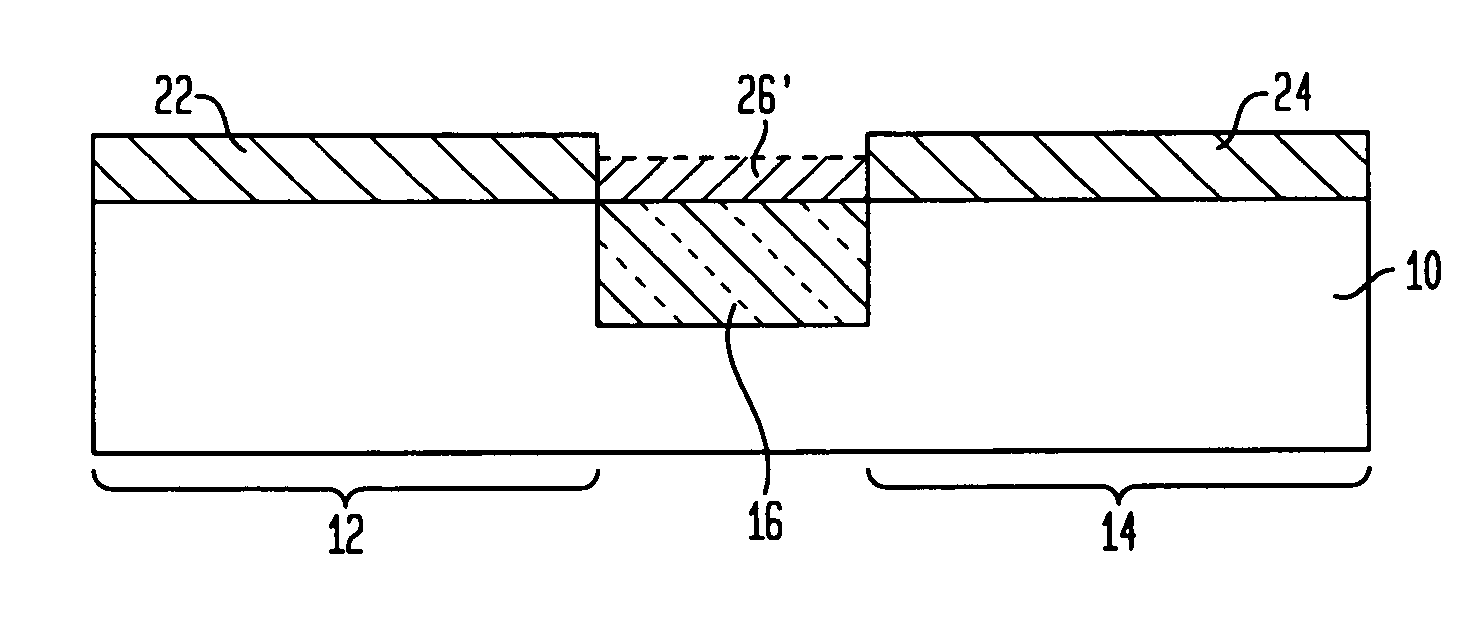
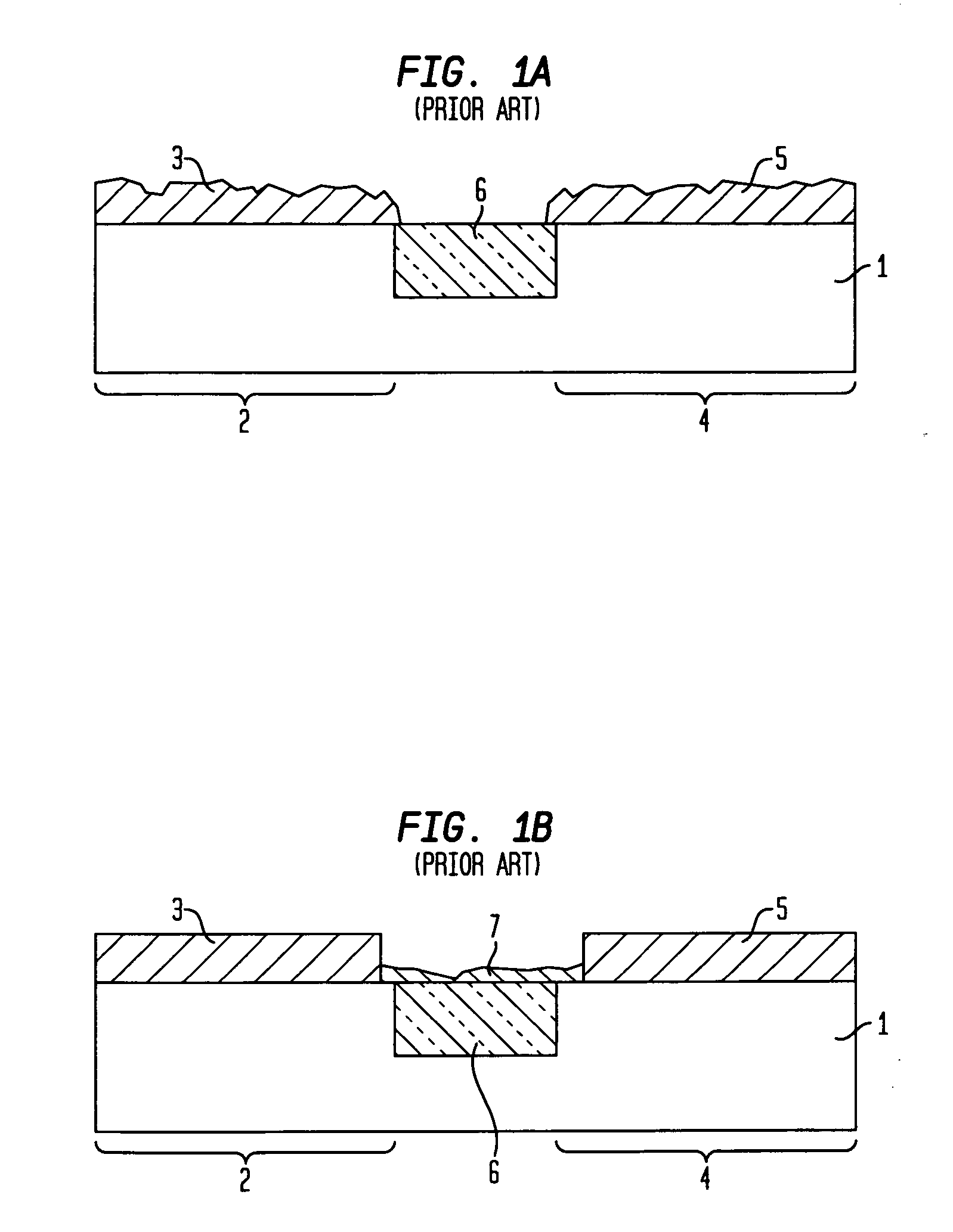
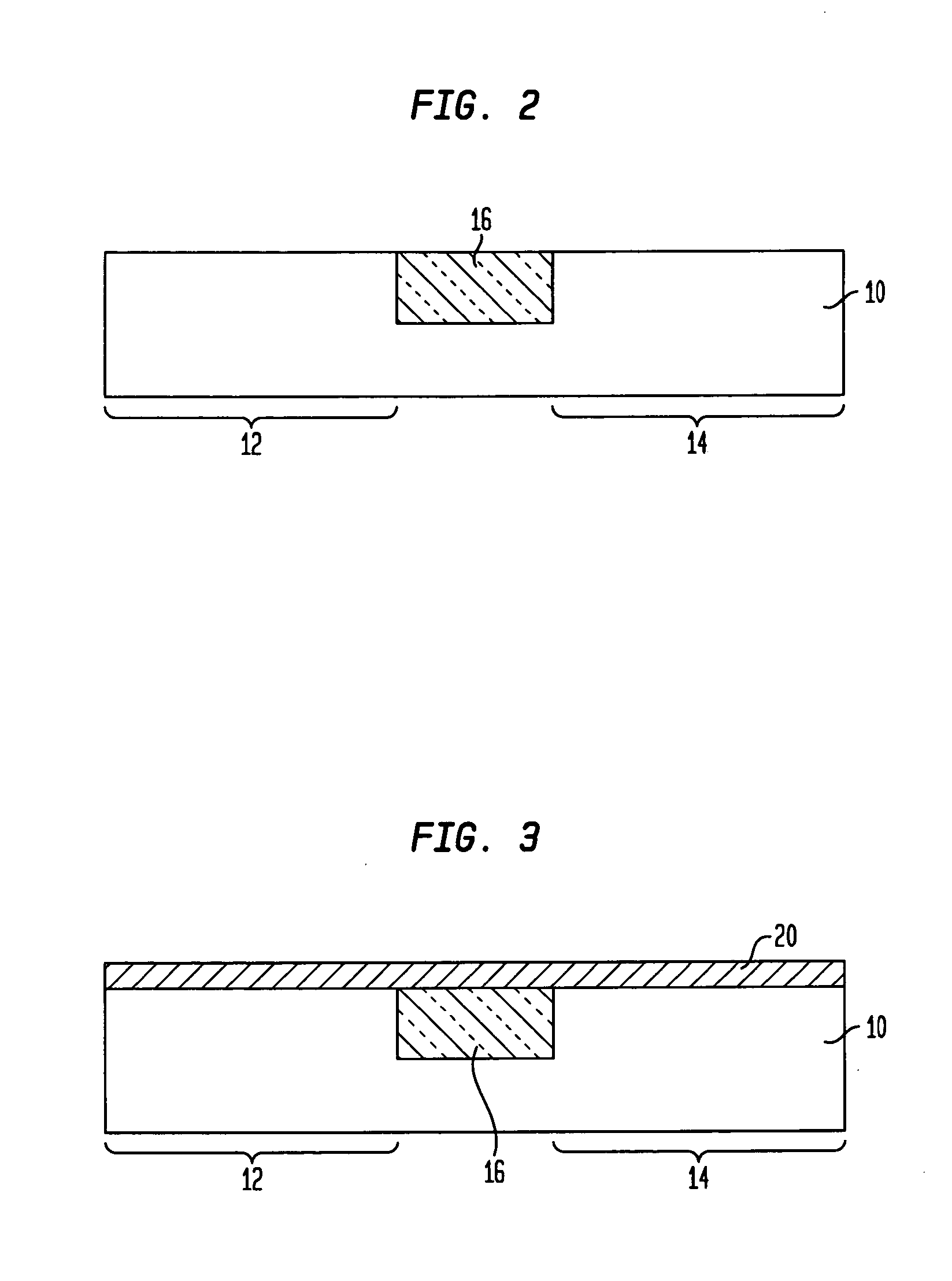
[0027] In the following description, numerous specific details are set forth, such as particular structures, components, materials, dimensions, processing steps and techniques, in order to provide a thorough understanding of the present invention. However, it will be appreciated by one of ordinary skill in the art that the invention may be practiced without these specific details. In other instances, well-known structures or processing steps have not been described in detail in order to avoid obscuring the invention.

[0028] It will be understood that when an element as a layer, region or substrate is referred to as being “on” or “over” another element, it can be directly on the other element or intervening elements may also be present. In contrast, when an element is referred to as being “directly on” or “directly over” another element, there are no intervening elements present. It will also be understood that when an element is referred to as being “connected” or “coupled” to anoth...


PUM

PropertyMeasurementUnit
Temperatureaaaaaaaaaa

Abstract

The present invention relates to a method for forming self-aligned metal silicide contacts over at least two silicon-containing semiconductor regions that are spaced apart from each other by an exposed dielectric region. Preferably, each of the self-aligned metal silicide contacts so formed comprises at least nickel silicide and platinum silicide with a substantially smooth surface, and the exposed dielectric region is essentially free of metal and metal silicide. More preferably, the method comprises the steps of nickel or nickel alloy deposition, low-temperature annealing, nickel etching, high-temperature annealing, and aqua regia etching.

Description

FIELD OF THE INVENTION [0001] The present invention generally relates to a method for forming self-aligned metal silicide contacts for semiconductor devices. More specifically, the present invention relates to a method for forming self-aligned metal silicide contacts for at least two silicon-containing semiconductor regions that are spaced apart from each other by an exposed dielectric region. BACKGROUND OF THE INVENTION [0002] The technological development of micro-sized semiconductor integrated circuit devices has required improved methods for making conductive contacts to the semiconductor impurity regions. Metal silicides have proven to be excellent contact materials, which can be readily formed in a self-aligned manner by a salicidation process. [0003] Formation of metal silicide contacts through the salicidation process typically involves the steps of depositing a thin metal layer (e.g., less than about 15 nm in thickness) that contains a silicide metal or metal alloy (i.e., a...

Claims


Application Information

Patent Timeline
IPC IPC(8): H01L21/44H01L21/302
CPCH01L21/28518C23F1/28C23F1/30C23F1/44H01L21/24H01L21/302
Inventor FANG, SUNFEIKNARR, RANDOLPHKRISHNAN, MAHADEVAIYERLAVOIE, CHRISTIANMO, RENEEPRANATHARTHIHARAN, BALASUBRAMANIANSTRANE, JAY
Owner TAIWAN SEMICON MFG CO LTD
Why Eureka
Try Eureka