
Method for repairing thin film transistor array substrate

a technology of array substrates and thin films, applied in the direction of electrical equipment, semiconductor devices, instruments, etc., can solve the problems of frequent production of dot defects or line defects, significant yield drop, etc., and achieve the effect of increasing the production yield of thin film transistor array substrates

Inactive Publication Date: 2007-11-08
CHUNGHWA PICTURE TUBES LTD
View PDF1 Cites 10 Cited by
  • Summary
  • Abstract
  • Description
  • Claims
  • Application Information

AI Technical Summary

Benefits of technology

[0008] Accordingly, at least one objective of the present invention is to provide a thin film transistor array substrate with the capacity for repairing any line defects including broken common lines, short-circuited common lines and data lines, broken scan lines and broken data lines therein. Ultimately, the production yield of the thin film transistor array substrate is increased.
[0009] At least a second objective of the present invention is to provide a method of repairing the aforementioned thin film transistor array substrate. The repairing method repairs a thin film transistor array substrate with line defects including broken common lines, short-circuited common lines and data lines, broken scan lines or broken data lines so that the production yield is increased.
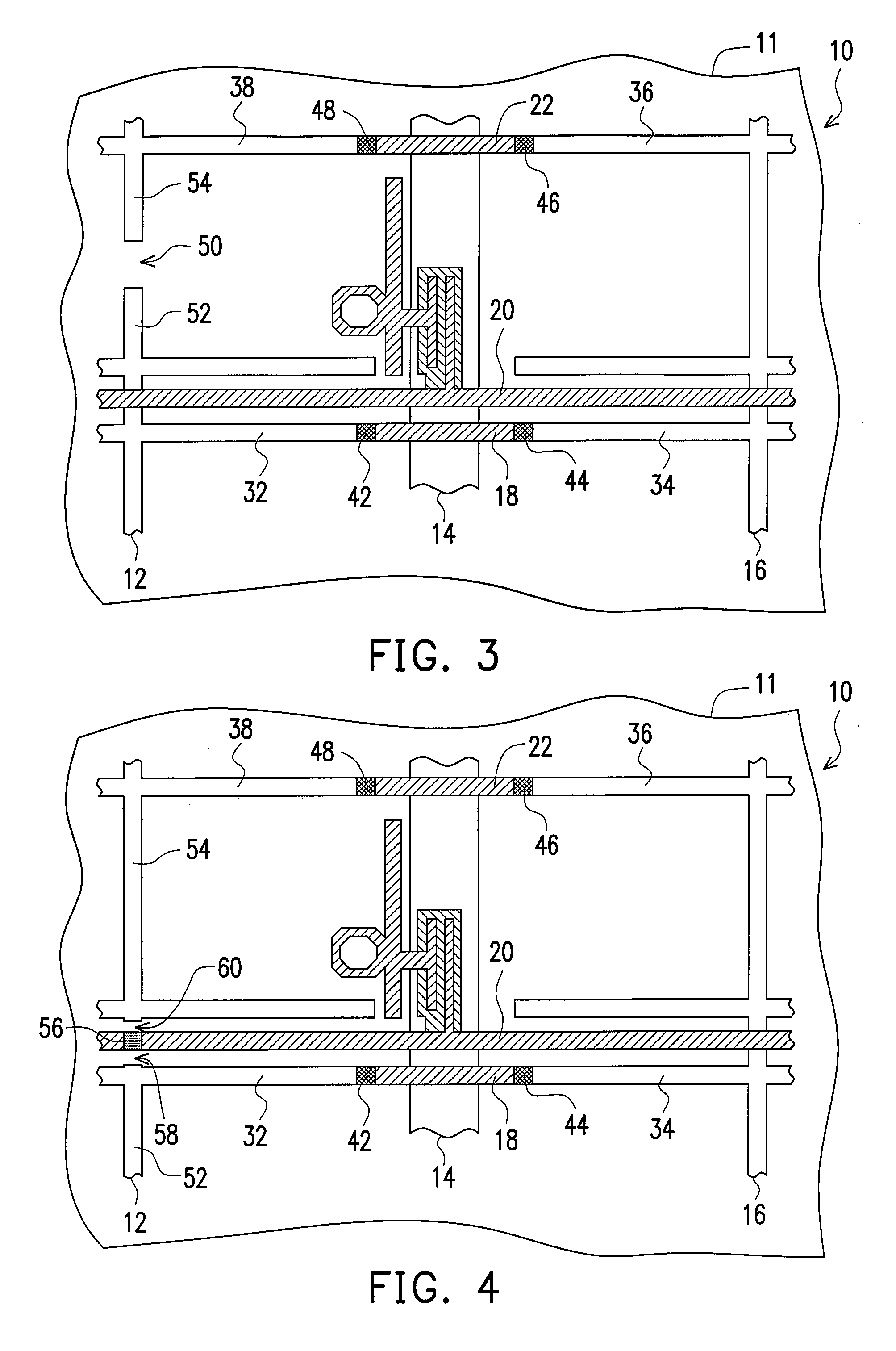
[0021] In the present invention, the repairing lines required to perform repairing operations and the data lines are formed at the same time. The repairing lines are formed over at least a scan line and laid in alternate locations with respect to the data line. Furthermore, the respective ends of each repairing line overlap partly with the two adjacent common lines on the respective sides of the scan line. By combining a laser welding operation for electrically connecting a repairing line with a common line together with a laser removal operation for isolating various connections, various line defects including broken common line, short-circuited common line and data line and broken scan line can be repaired.
[0022] In addition, the branches of the common lines, each has a protruding portion in the present invention. Furthermore, the protruding portion extends to an area above a corresponding data line and overlaps partly with the data lines. During a repair operation, through a laser welding operation for electrically connecting a data line with a common line together with a laser removal operation for isolating various connections, a line defect caused by a broken data line can be repaired.

Problems solved by technology

Although the conventional cathode ray tube (CRT) displays still have some advantages, bulkiness and high operating power are some major factors that render its replacement by more versatile device inevitable.
In the process of fabricating the thin film transistor array substrate, dot defects or line defects are frequently produced.
When the aforementioned line defects occur in the thin film transistor array substrate, there will be a significant drop in the yield if the abnormal portion is not repaired.

Method used


Image

  • Method for repairing thin film transistor array substrate
  • Method for repairing thin film transistor array substrate
  • Method for repairing thin film transistor array substrate

Examples


first embodiment

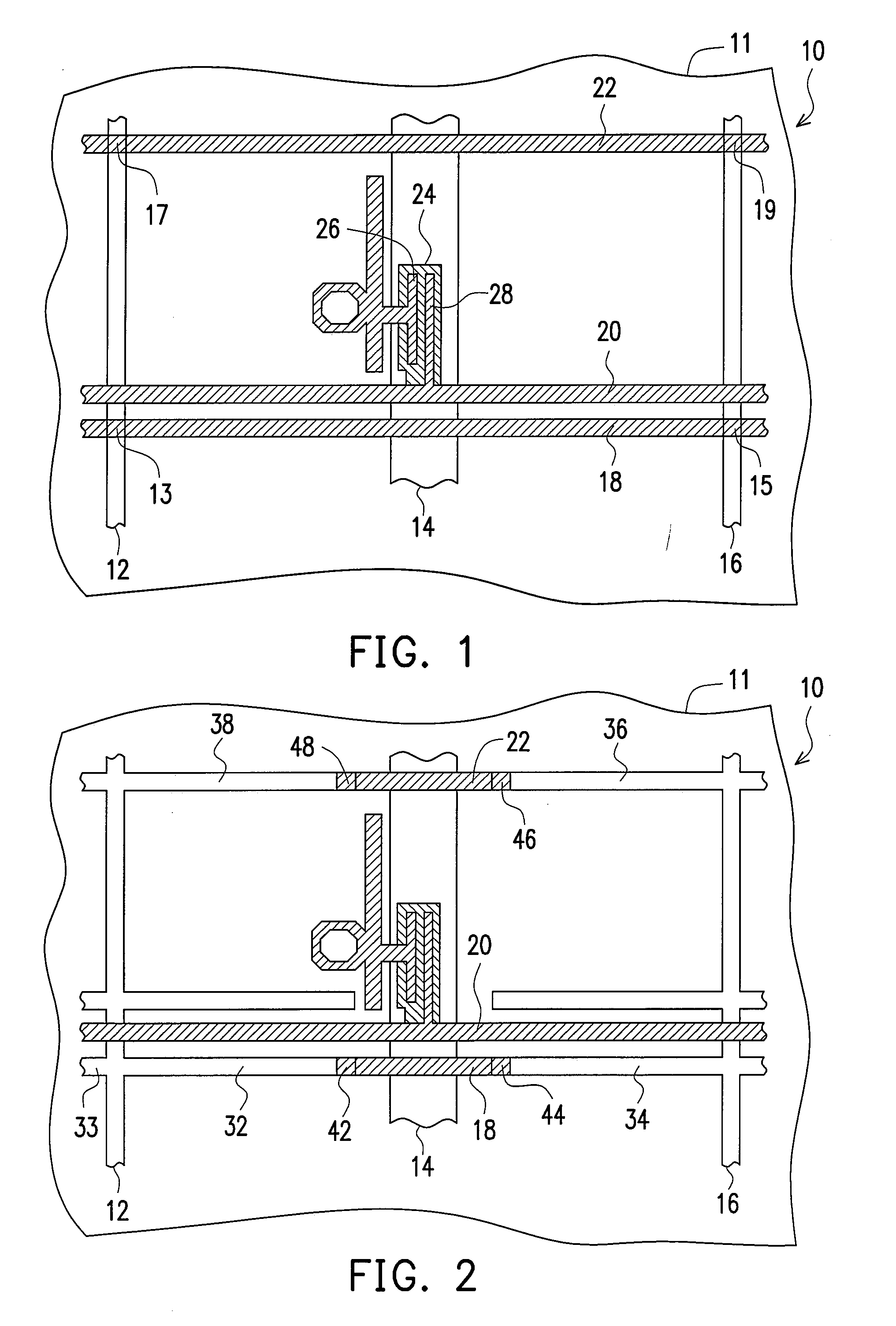
[0034]FIG. 1 is a top view showing the local structure of a thin film transistor array substrate according to the present invention. As shown in FIG. 1, a first common line 12, a scan line 14 and an adjacent second common line 16 of the thin film transistor array substrate 10 are disposed in parallel and alternately laid on a glass substrate 11, for example. A first repairing line 18, a data line 20 and a second repairing line 22 are alternately disposed over the glass substrate 11. The first repairing line 18 and the second repairing line 22 are disposed over the scan line 14. Furthermore, the two ends of the first repairing line 18 form partial overlaps 13 and 15 with the two adjacent common lines 12 and 16 on each side of the scan line 14. Similarly, the two ends of the second repairing line 22 form partial overlaps 17 and 19 with the two adjacent common lines 12 and 16 on each side of the scan line 14. A source 26 and a drain 28 of the thin film transistor are disposed over a se...

third embodiment

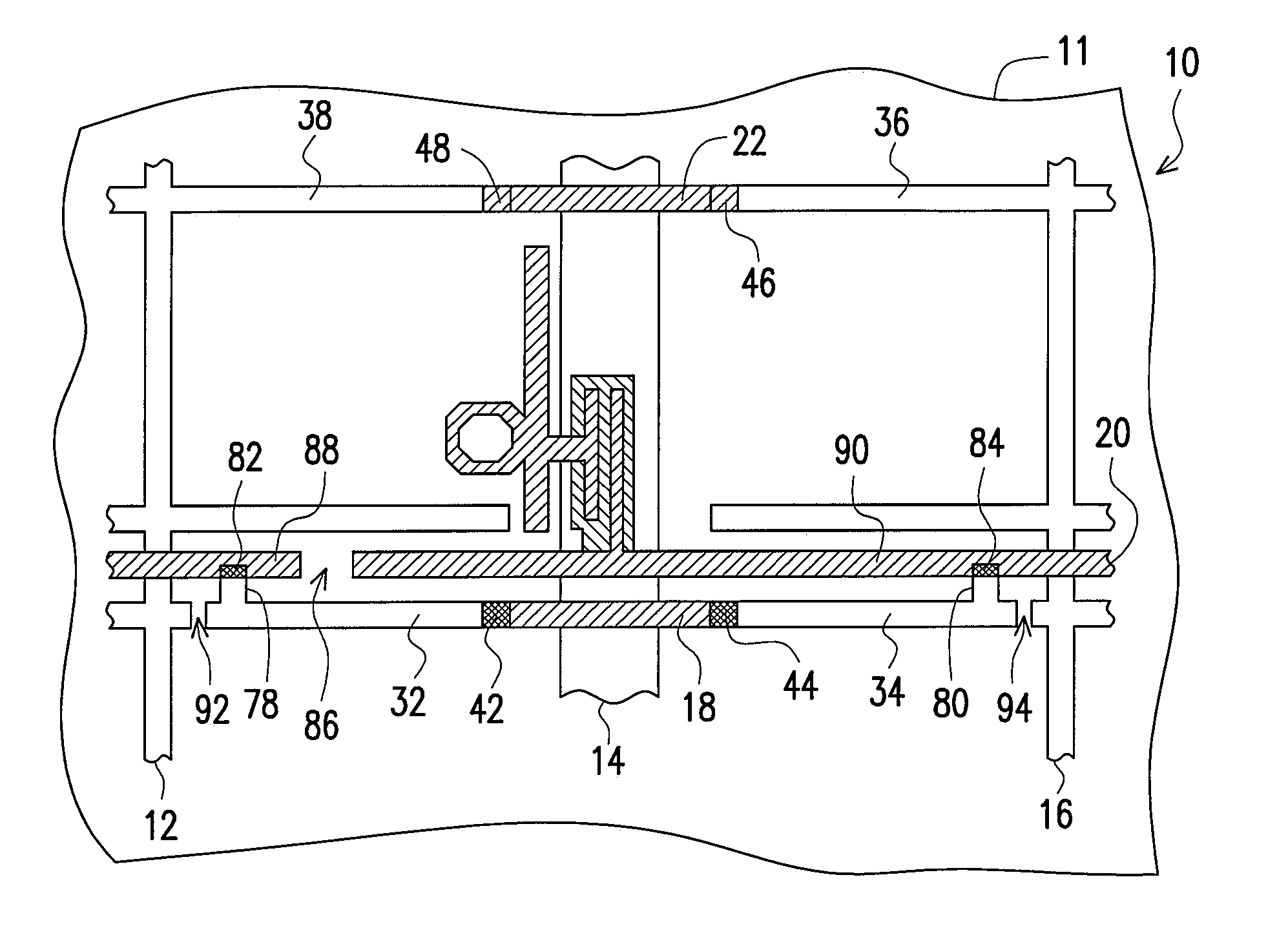
[0042] In the following, a third embodiment for repairing a broken data line is disclosed. However, this method should by no means limit the scope of the present invention. FIG. 7 is a top view of the local structure of a thin film transistor array substrate showing the method for repairing a broken data line according to the present invention. As shown in FIG. 7, a data line 20 in the thin film transistor array substrate 10 has a broken point 86. Hence, the data line 20 is divided into a seventh portion 88 and an eighth portion 90 that are electrically isolated from each other. The repairing method includes performing a laser welding from the back of the thin film transistor array substrate 10 to fuse the seventh portion 88 and a first protruding portion 78 together through a seventh overlap portion 82. Hence, the seventh portion 88 and the first branch 32 are electrically connected through the seventh overlap portion 82. Similarly, the first branch 32 and the first repairing line ...


PUM


Abstract

A thin film transistor array substrate and method for repairing the same are provided. Repairing lines are formed when the data lines on the thin film transistor array substrate are defined. Furthermore, the protruding portions and branches of common lines overlap with the repairing lines and the data lines respectively. The repairing method includes performing a laser welding operation to connect the common line with the data line, the repairing line or a scan line as well as removing a portion of the lines by laser. Thus, the thin film transistor array substrate and repairing method thereof can repair line defects and increase the manufacturing yield.

Description

CROSS-REFERENCE TO RELATED APPLICATION [0001] This application is a divisional of a prior application Ser. No. 11 / 214,758, filed Aug. 29, 2005, now allowed. The entirety of each of the above-mentioned patent application is hereby incorporated by reference and made a part of this specification.BACKGROUND OF THE INVENTION [0002] 1. Field of the Invention [0003] The present invention relates to an array substrate and method for repairing the same. More particularly, the present invention relates to a thin film transistor array substrate and method for repairing the same. [0004] 2. Description of the Related Art [0005] To fit into our modem lifestyle, the size and weight of video or imaging equipment are decreasing at a phenomenal pace. Although the conventional cathode ray tube (CRT) displays still have some advantages, bulkiness and high operating power are some major factors that render its replacement by more versatile device inevitable. Nowadays, thin film transistor liquid crystal...

Claims


Application Information

Patent Timeline
Patent Type & Authority Applications(United States)
IPC IPC(8): H01L21/00
CPCG02F1/136259H01L27/124G02F2001/136263G02F1/136263
Inventor CHEN, CHIN-SHENGLIU, CHIH-HUNGHUNG, CHIEN-HSINGHUANG, KUN-YUAN
Owner CHUNGHWA PICTURE TUBES LTD
Learn More