

Manufacturing method of semiconductor device having organic semiconductor film
a manufacturing method and semiconductor technology, applied in semiconductor devices, electrical equipment, material nanotechnology, etc., can solve the problems of increasing parasitic capacitance or performance fluctuation, increasing the cost and time it takes in the apparatus for each of the steps, and difficult manufacturing of fine tfts
- Summary
- Abstract
- Description
- Claims
- Application Information
AI Technical Summary
Benefits of technology
Problems solved by technology
Method used
Image

Examples
first embodiment
ng a Solution Layer for Electrode From the Rear Face of a Substrate Using an Opaque Gate Electrode as a Mask Region
[0065] As described above, in the first basic embodiment, the ends of the pair of both source and drain electrodes on the side of the gate electrode are set by exposure from the rear face of a substrate using the gate electrode as a mask region. More preferably, the channel portion, the insulator, the gate electrode, and the source and drain electrodes are formed by the printing method.
[0066] In this case, the specific procedure for forming the electrode and forming the organic semiconductor film typically includes the following two procedures. At first, the step of forming the organic semiconductor film is applied before the step of forming the electrode material layer. Secondly, the step of forming the organic semiconductor film is applied after the step of forming the electrode material layer.
[0067] Further, it is more preferred for attaining the purpose of the inv...
second embodiment
ng the Difference of Property to the Coating Solution Between the Gate Insulator and the Surface of the Substrate
[0097] The second embodiment provides a method of manufacturing a semiconductor device having a thin organic film transistor having, on a substrate, a channel portion comprising an organic semiconductor, an insulator in contact with the channel portion, a gate electrode in contact with the insulator, and a pair of source and drain electrodes spaced apart by the channel portion, in which the property with a liquid, that is, whether it is hydrophilic or hydrophobic is made different between the surface of the substrate and the surface of the gate insulator from each other, so that the solution of the source electrode and the drain electrode materials are repelled selectively from a portion on the gate insulator, and the ends of both of the pair of source and drain electrodes on the side of the gate electrode are set.
[0098] The material for the surface of the substrate and ...
example 1
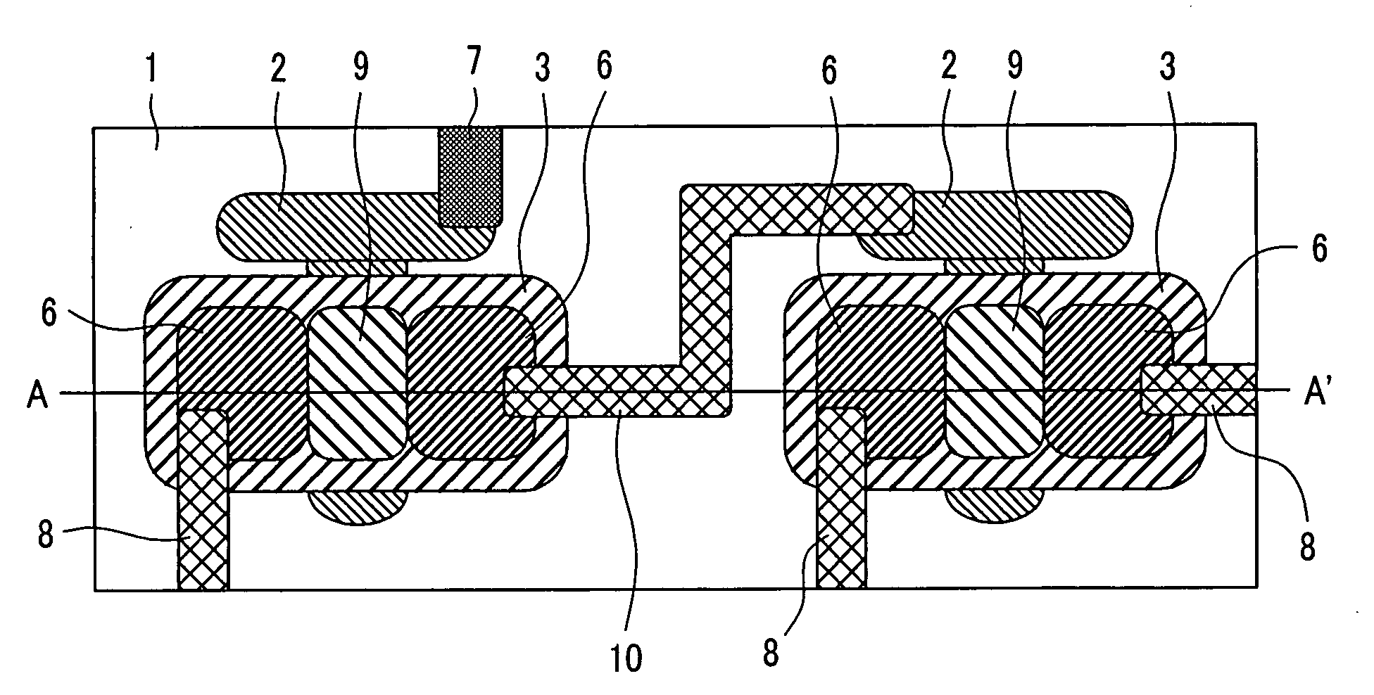
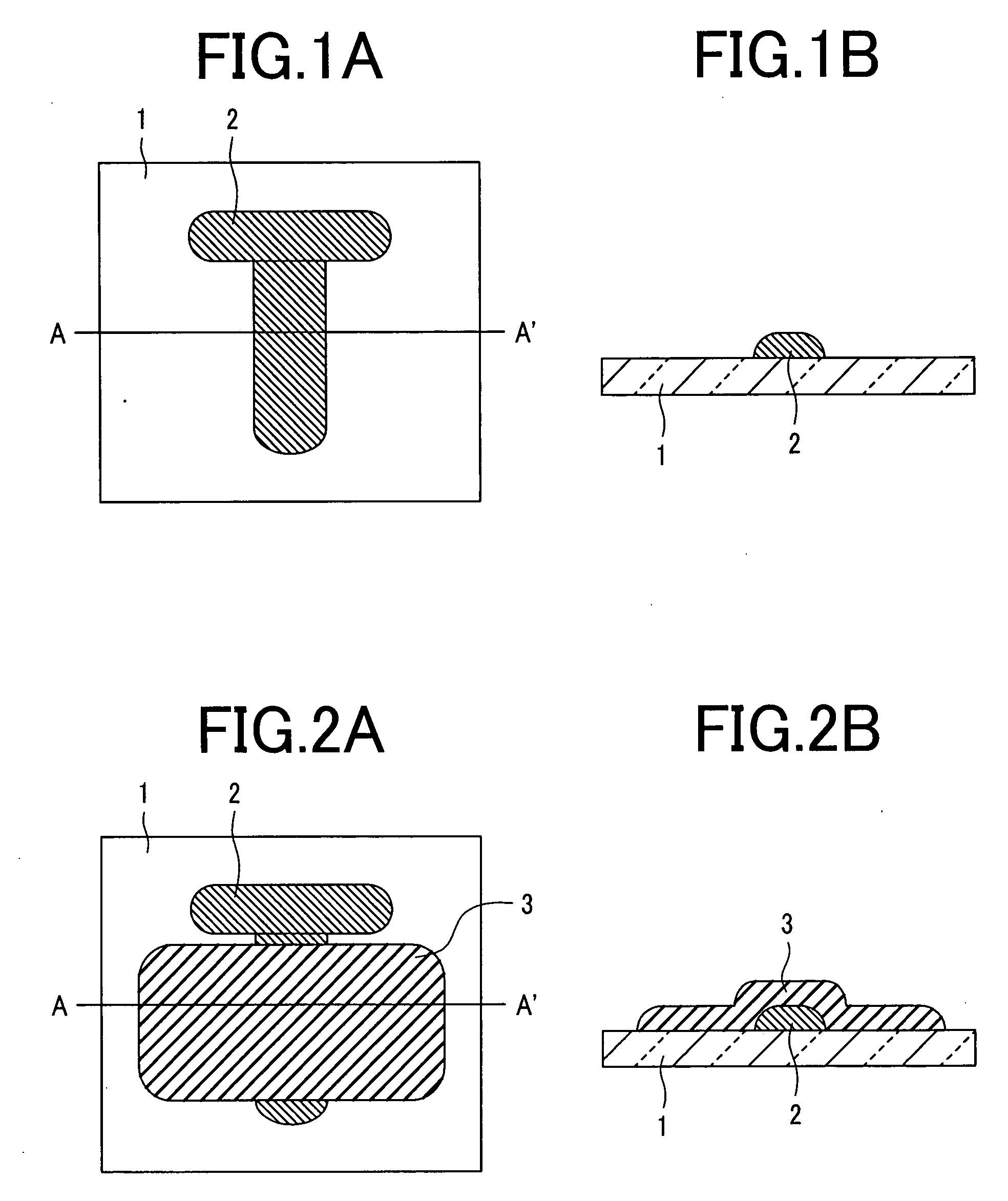
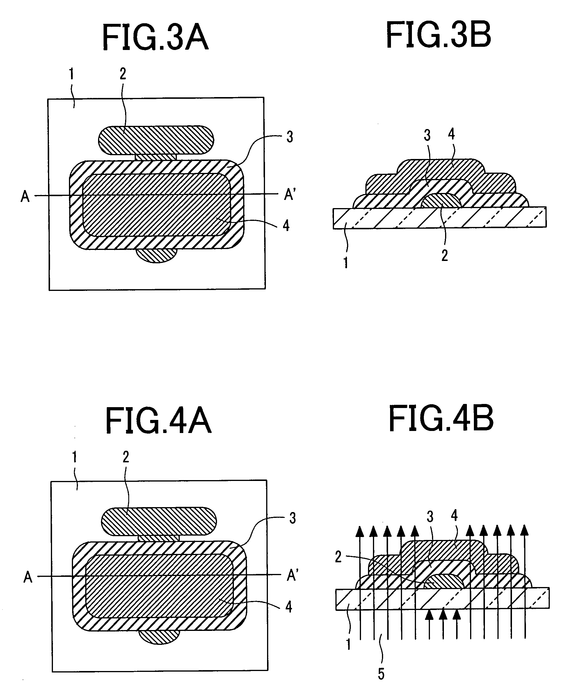
[0173]FIGS. 1A and 1B to FIGS. 8A and 8B are plan views and cross sectional views, respectively, of a device in the order of manufacturing steps of this example for forming source and drain electrodes by exposure from the rear face of a substrate. In each of FIGS. 1A and 1B to FIGS. 8A and 8B, (A) is an upper plan view and (B) is a cross sectional view along line A-A′ in (A). In the upper plan view and the cross sectional view of the device shown in the order of the manufacturing steps in the present specification, (A) is an upper plan view and (B) is a cross sectional view in each of the drawings.
[0174] A gate electrode shape having a line width of 20 μm was printed by using polyethylene terephthalate as an organic compound for a transparent substrate 1 and using gold-nano-particles dispersed in a toluene solution as an ink by an ink jet printing method to form a gold gate electrode 2 by over heating at 120° C. for 5 min (upper plan view: FIG. 1A, and cross sectional view: FIG. 1B...
PUM
 Abstract
Description
Claims
Application Information