Insulated gate semiconductor device

a semiconductor device and gate technology, applied in the direction of semiconductor devices, electrical equipment, transistors, etc., can solve the problems of reducing the operation region (a disposition area of the transistor cell) of the transistor, deteriorating the reverse breakdown voltage of the drain source, and unable to obtain the desired reverse breakdown voltag

Active Publication Date: 2007-11-15
SEMICON COMPONENTS IND LLC
View PDF11 Cites 28 Cited by
  • Summary
  • Abstract
  • Description
  • Claims
  • Application Information

AI Technical Summary

Benefits of technology

[0024] The invention also provides an insulated gate semiconductor device that includes a semiconductor substrate of a first general conductivity type, a plurality of gate electrodes formed on the semiconductor substrate and arranged in a first stripe pattern, a plurality of channel regions of a second general conductivity type formed on the semiconductor substrate and arranged in a second stripe pattern, the first and second stripe patterns being oriented in a first direction, a first insulating film disposed between the channel regions and the gate electrodes, a plurality of source regions of the first general conductivity type formed in corresponding channel regions and arranged in a third stripe pattern oriented in the first direction, a second insulating film disposed on the gate electrodes, a gate pad electrode disposed on the second insulating film, a gate extraction electrode disposed in a periphery of the semiconductor substrate and connecting the gate electrodes and the gate pad electrode, and a high-concentration region of the second general conductivity type formed on the substrate below the gate extraction electrode and connected with the channel regions. In this device part of the channel regions, part of the gate extraction electrode and part of the gate electrodes are located below the gate pad electrode and corresponding portion of the second insulating film.

Problems solved by technology

Accordingly, there is a problem that a desired drain-source reverse breakdown voltage cannot be obtained.
In such a case, the pattern of the p+ type impurity region 49 shown in FIGS. 7A and 7B also has a problem that the drain-source reverse breakdown voltage is deteriorated.
Consequently, there is a problem that the operation region (a disposition area of the transistor cells) has to be reduced.

Method used


Image

  • Insulated gate semiconductor device
  • Insulated gate semiconductor device
  • Insulated gate semiconductor device

Examples


first embodiment

[0035] FIGS. 1 to 3 show the present invention.

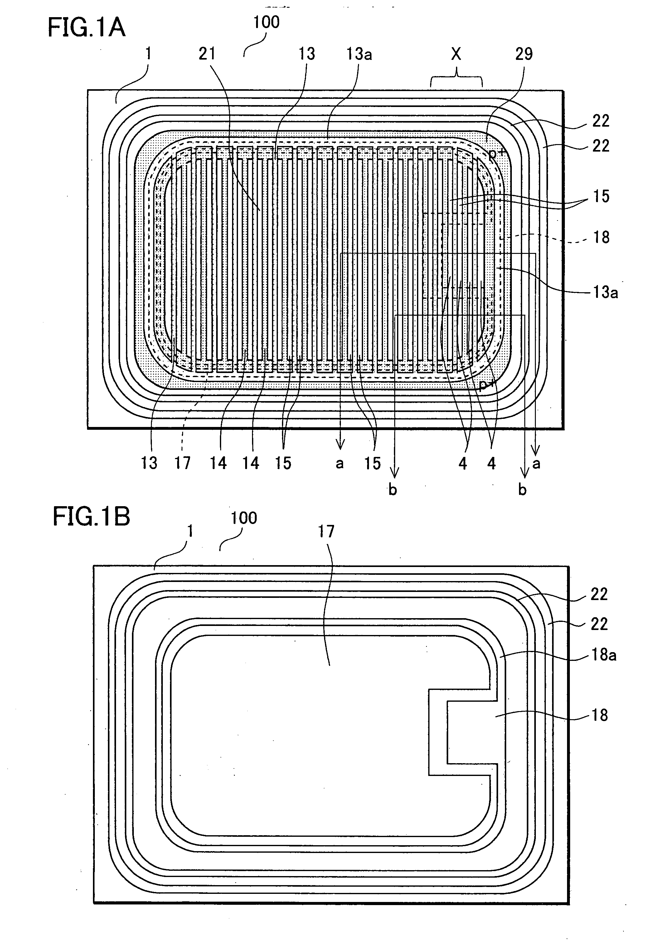
[0036]FIGS. 1A and 1B are plan views of a chip of a MOSFET according to the first embodiment of the present invention. FIG. 1A is a plan view in which interlayer insulating films are omitted and a metal electrode layer (a source electrode, a gate pad electrode and a gate wiring) is indicated by a broken line. FIG. 1B is a plan view showing patterns of the source electrode, the gate pad electrode and the gate wiring.

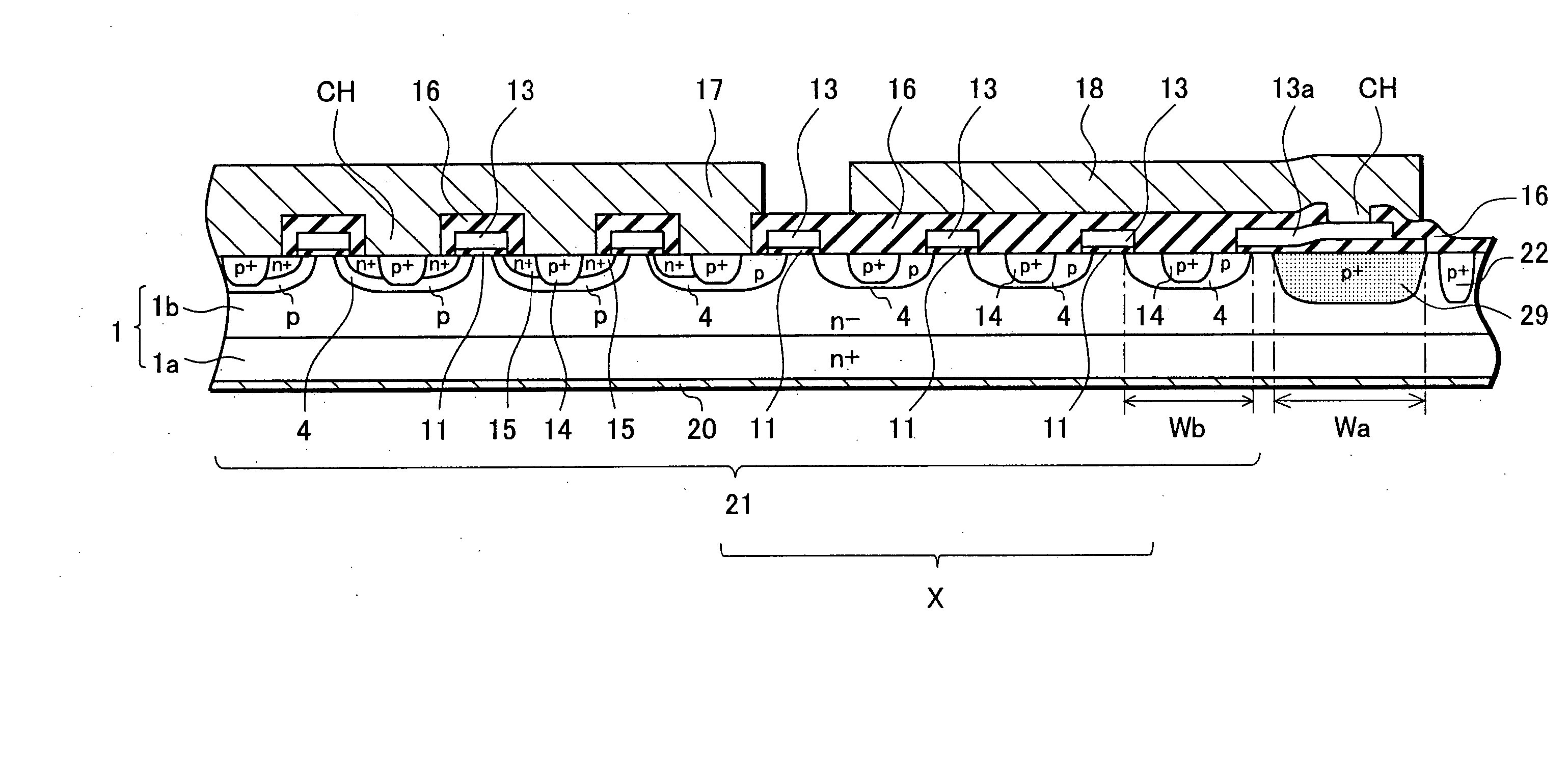
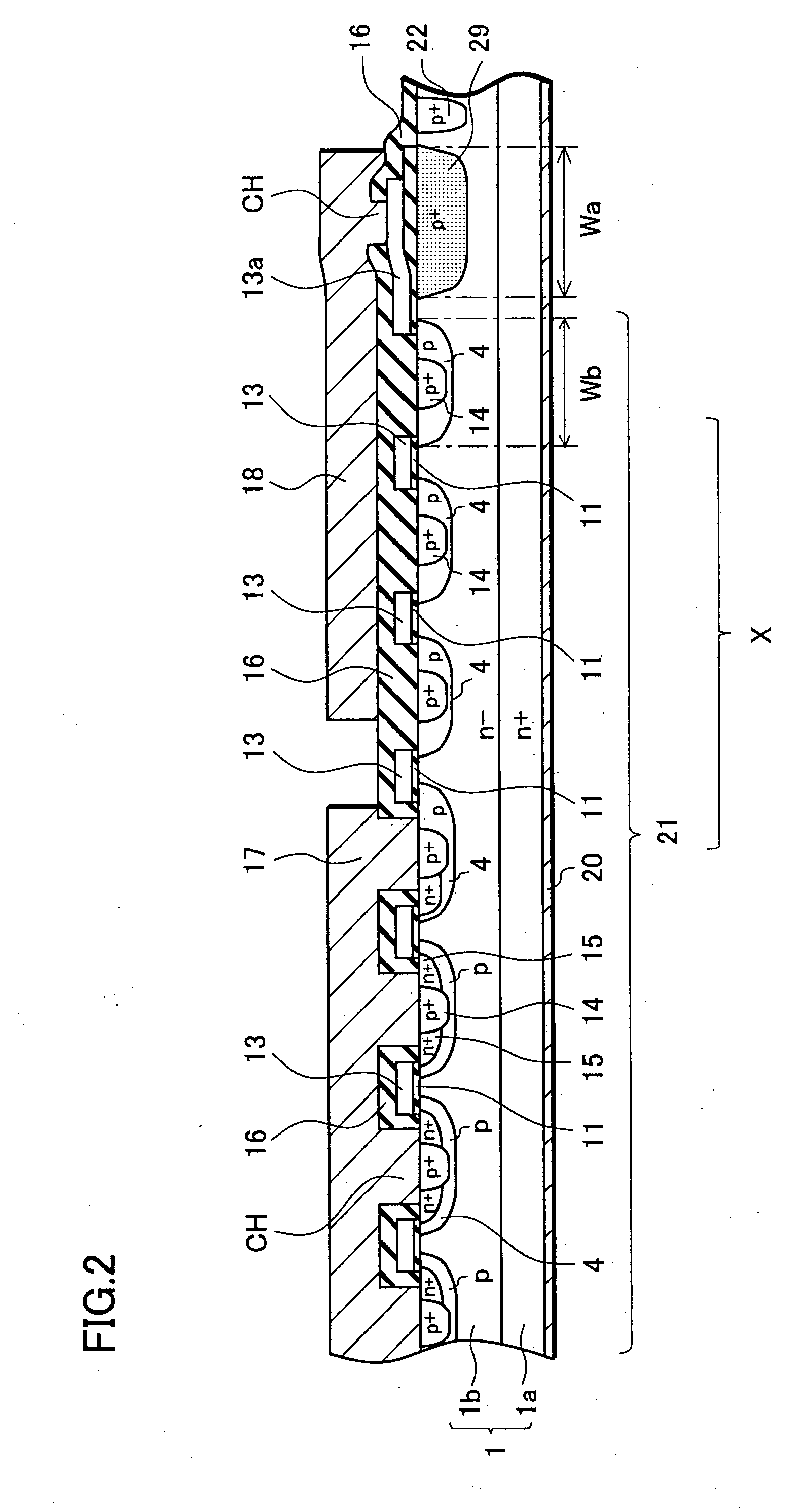
[0037] A MOSFET 100 of the first embodiment of the present invention includes an n type semiconductor substrate 1, channel regions 4, first insulating films 11, gate electrodes 13, source regions 15, body regions 14, second insulating films 16, a gate pad electrode 18 and a source electrode 17.

[0038] As shown in FIG. 1A, the gate electrodes 13 are provided in a stripe pattern on the n type semiconductor substrate 1 with gate oxide films (not shown here) interposed therebetween, which are to be the first insulating films pro...


PUM


Abstract

Channel regions and gate electrodes are also disposed continuously with transistor cells below a gate pad electrode. The transistor cells are formed in a stripe pattern and allowed to contact a source electrode. In this way, the channel regions and the gate electrodes, which are positioned below the gate pad electrode, are kept at a predetermined potential. Thus, a predetermined drain-source reverse breakdown voltage can be secured without providing a p+ type impurity region on the entire surface below the gate pad electrode.

Description

BACKGROUND OF THE INVENTION [0001] This application claims priority from Japanese Patent Application No. 2006-131820, filed May 10, 2006, the content of which is incorporated herein by reference in its entirety. [0002] 1. Field of the Invention [0003] The present invention relates to an insulated gate semiconductor device, and more particularly relates to an insulated gate semiconductor device which can maintain a high reverse breakdown voltage by securing a sufficient operation region area. [0004] 2. Description of the Related Art [0005] In a conventional insulated gate semiconductor device, no transistor cell is disposed below a gate pad electrode. This technique is described for instance in Japanese Patent Application Laid-open Publication No. 2002-368218. [0006] In addition, a protection diode having a plurality of series-connected pn junctions, for example, may be disposed below a gate pad electrode. Otherwise, a diffusion region of high-concentration impurities may also be for...

Claims


Application Information

Patent Timeline
Patent Type & Authority Applications(United States)
IPC IPC(8): H01L29/94
CPCH01L27/088H01L29/0619H01L29/0696H01L29/1095H01L29/7813H01L29/7395H01L29/7397H01L29/7811H01L29/42372H01L2224/0603
Inventor ISHIDA, HIROYASUNOGUCHI, YASUNARI
Owner SEMICON COMPONENTS IND LLC
Why Eureka
Try Eureka