Manufacturing method for cilicon epitaxial wafer for 6'' VDMOS tube

A technology of silicon epitaxial wafer and manufacturing method, which is applied in semiconductor/solid-state device manufacturing, electrical components, circuits, etc., can solve the problems of increasing parameter control difficulty, high central resistivity of epitaxial wafer, and large edge.

Active Publication Date: 2007-10-03
NANJING GUOSHENG ELECTRONICS
View PDF1 Cites 22 Cited by
  • Summary
  • Abstract
  • Description
  • Claims
  • Application Information

AI Technical Summary

Problems solved by technology

The result is: high resistivity in the center of the epitaxial wafer, low resistivity at the edge, small center and large edge in the transition zone of the epitaxial wafer
When the device is manufactured, the breakdown voltage BVDS is small in the middle and t

Method used


Image

  • Manufacturing method for cilicon epitaxial wafer for 6'' VDMOS tube
  • Manufacturing method for cilicon epitaxial wafer for 6'' VDMOS tube
  • Manufacturing method for cilicon epitaxial wafer for 6'' VDMOS tube

Examples


Embodiment Construction

[0017] The specific embodiments of the present invention will be described in detail below in conjunction with the accompanying drawings:

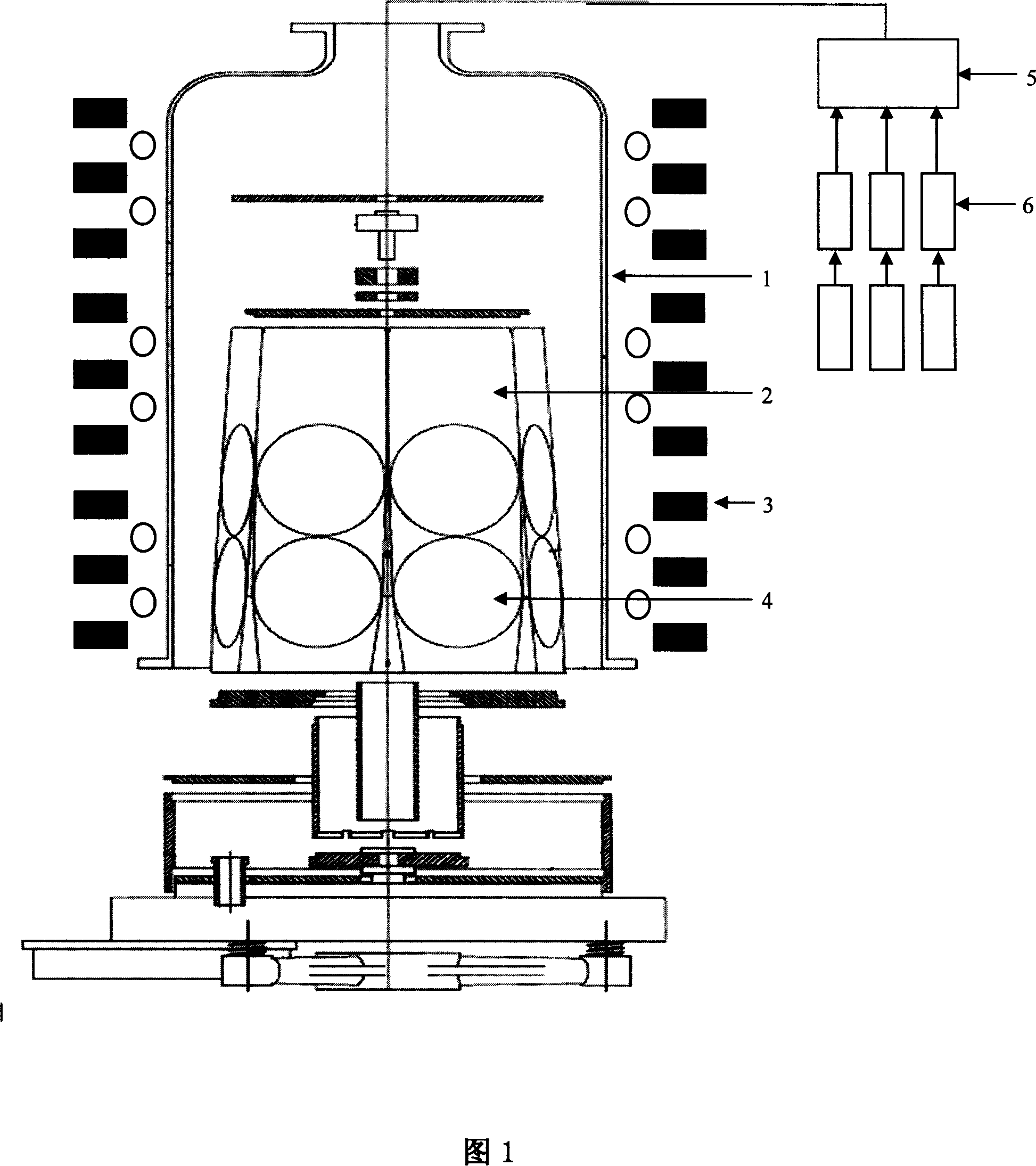
[0018] The equipment used in the present invention is a PE-2061S epitaxial furnace produced in Italy, as shown in Figure 1. The base is a high-purity graphite surface that has been cracked and encapsulated with high-purity SiC, heated by high-frequency induction, and the hydrogen purifier is adsorbed by molecular sieves. is 99.99999%. In the figure: 1 is a quartz reactor; 2 is a graphite base; 3 is a heating coil; 4 is a silicon substrate sheet; 5 is a gas distribution system; 6 is a gas flow control system.

[0019] Reactor and substrate cleaning: The quartz bell and the quartz support must be carefully cleaned before high-resistance epitaxy to remove the impurity atoms and residues adsorbed on the inner wall of the quartz reactor and quartz parts.

[0020] Graphite susceptor treatment: Before growing epitaxial wafers, the susceptor must...


PUM


Abstract

The present invention relates to a preparation method of silicon epitaxial wafer for power VDMOS tube. Firstly, selection and usage of substrate are important, the selected substrate not only can meet the requirements for device, but also can meet the requirements for epitaxy. Its preparation method includes the following steps: selecting proper gas corrosion flow and gas corrosion time, reducing concentration of gas corrosion impurity in epitaxial reactor so as to reduce self-doping in epitaxial growth process; first layer epitaxial growth, on the substrate surface with high concentration utilizing lower temperature to grow a layer of purity epitaxial layer, encapsulating substrate surface and edge, controlling its growth temperature, growth rate and epitaxial time so as to make encapsulating layer obtain ideal effect, at the same time, selecting proper epitaxial condition to make the deformation of epitaxial wafer be minimum; and second layer epitaxial growth, utilizing tower temperature to grow a layer of epitaxial layer whose resistivity and thickness can meet requirements for device.

Description

1. Technical field [0001] The present invention relates to a silicon epitaxial wafer, in particular, to a manufacturing method of a silicon epitaxial wafer for 6" VDMOS power tube. 2. Background technology [0002] Power MOSFET is a voltage-controlled unipolar transistor, which controls the drain current through the gate voltage, so one of its notable features is that the driving circuit is simple and the driving power is small; it is only conducted by majority carriers, and there are no minority carriers. Storage effect, good high-frequency characteristics, operating frequency up to 100kHz or more, the highest frequency among all power electronic devices, so it is most suitable for high-frequency applications such as switching power supply, high-frequency induction heating; no secondary breakdown problem, safe work Wide area, strong damage resistance. It adopts the fine processing technology of VLSI and uses N / N+ epitaxial structure, so it has special requirements and stan...

Claims


Application Information

Patent Timeline
IPC IPC(8): H01L21/20
Inventor 马林宝
Owner NANJING GUOSHENG ELECTRONICS
Why Eureka
Try Eureka