
Method and structure for creation of a metal insulator metal capacitor

Active Publication Date: 2007-11-15
GLOBALFOUNDRIES US INC
View PDF14 Cites 2 Cited by
  • Summary
  • Abstract
  • Description
  • Claims
  • Application Information

AI Technical Summary

Benefits of technology

[0012] The invention solves the aforementioned problems associated with prior art capacitors. More specifically, the invention prevents yield failures associated with high-K dielectric through the use of a protective layer. The invention is dielectric independent. Therefore, both high and low-K dielectric materials can be used as insulator without negatively affecting yield.
[0013] For at least the foregoing reasons, the invention improves capacitor technology.

Problems solved by technology

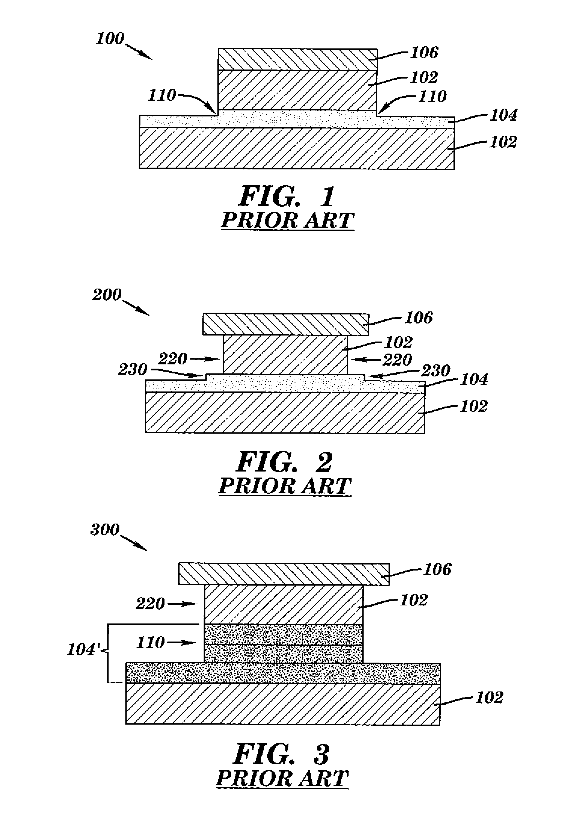
One disadvantage associated with prior art MIM capacitors are edge defects that occur in the insulator at the interface with the top metal layer.
Edge defects result in early device failure.
One disadvantage of a MIM capacitor with pullback 200, however is that such construction only works with an insulator 104 comprised of low-K dielectric, e.g. SiN.
Such construction, however, does not work with an insulator 104 comprised of high-K dielectric.
Such insulator 104 results in edge defects and increased leakage.

Method used


Image

  • Method and structure for creation of a metal insulator metal capacitor
  • Method and structure for creation of a metal insulator metal capacitor
  • Method and structure for creation of a metal insulator metal capacitor

Examples


Embodiment Construction

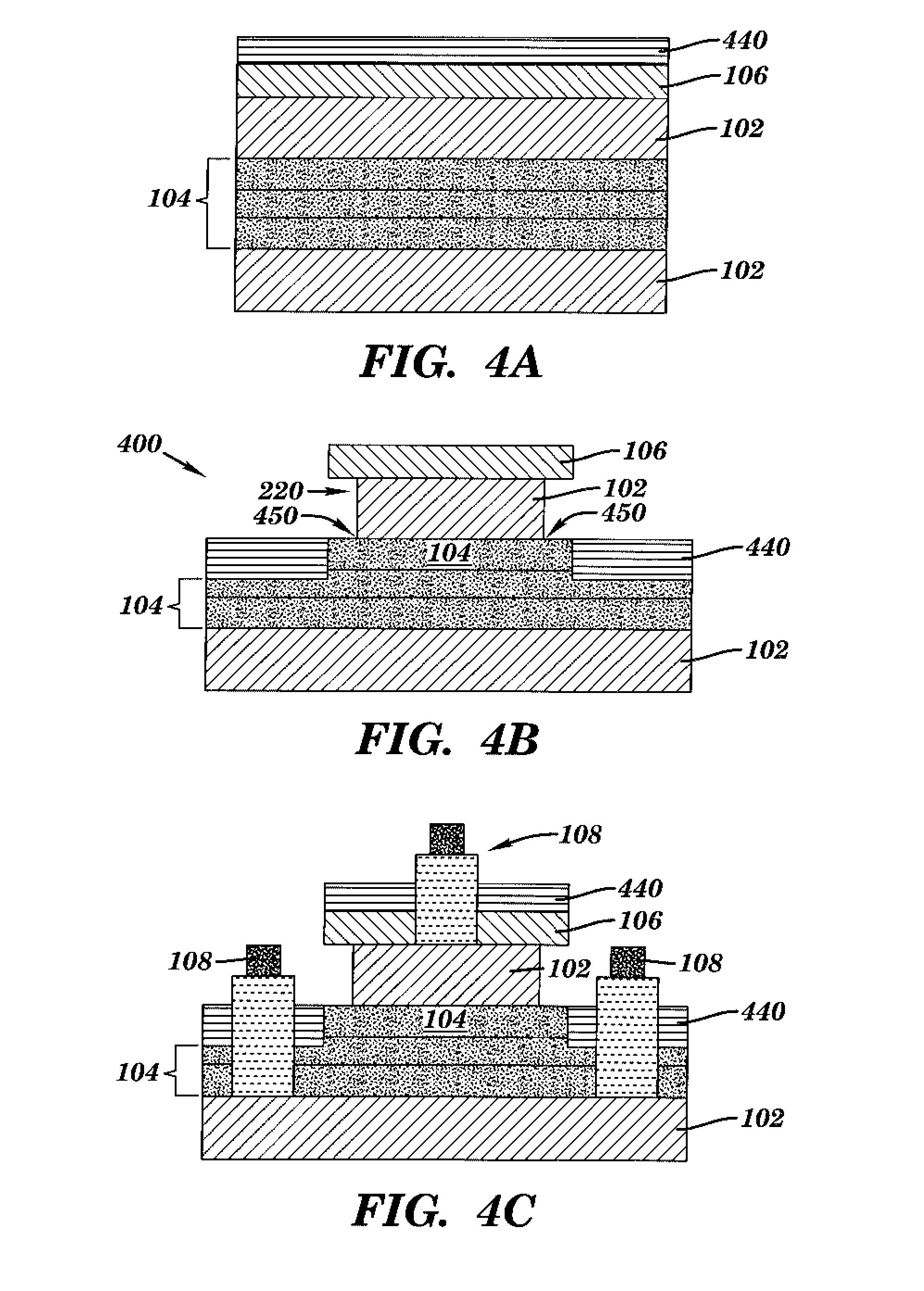
[0024] The invention will now be described with reference to the accompanying figures. In the figures, various aspects of the structures have been depicted and schematically represented in a simplified manner to more clearly describe and illustrate the invention.

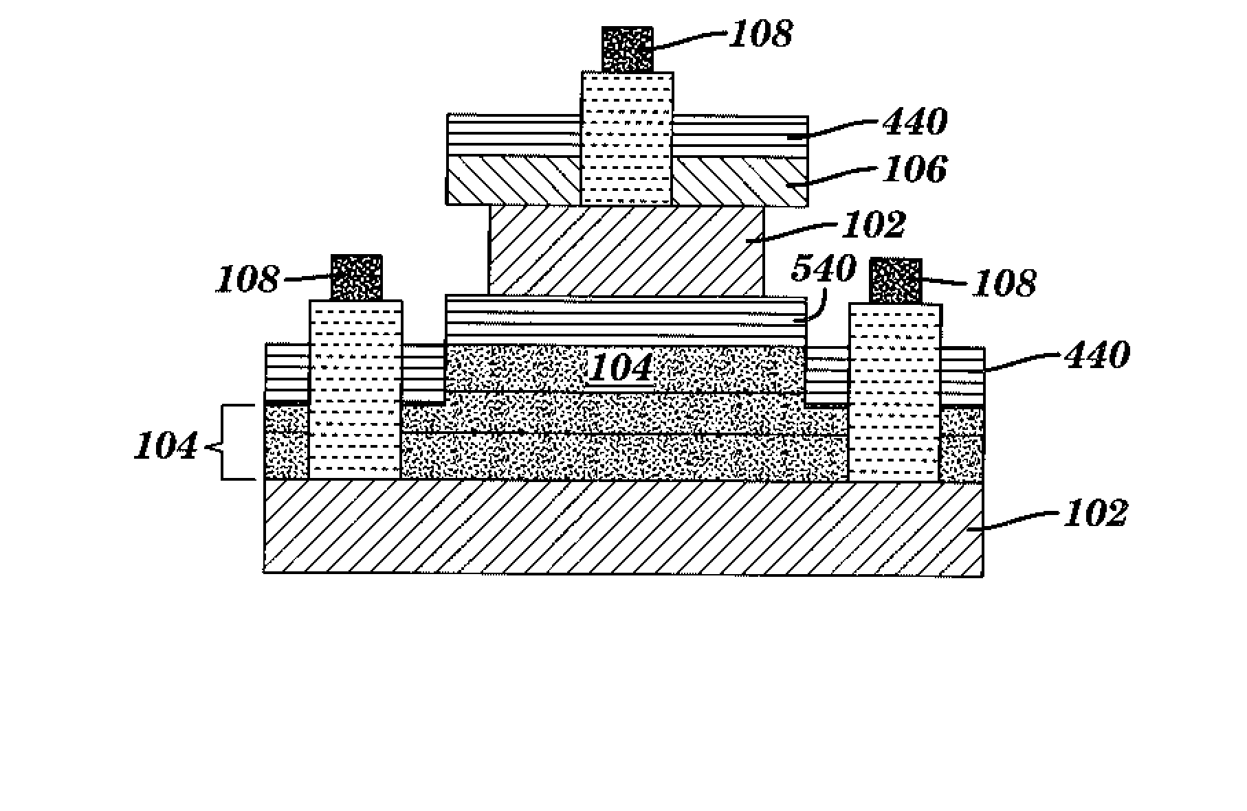
[0025] By way of overview and introduction, the embodiments of the invention are directed to a capacitor and method for creation of the same. All embodiments comprise a protective layer deposited either adjacent an insulator upon which the second conductive layer is deposited or on an insulator upon which the second conductive layer is deposited. In all embodiments, the length of the top conductive layer is shorter than the length of the insulator 104 at the interface with the conductive layer 102 (first embodiment) or protective layer 540 (second embodiment).

[0026] A first embodiment of the invention will be described with reference to the FIGS. 4A-C, which depict the formation of an improved capacitor, and more specifica...


PUM


Abstract

The invention is directed to an improved capacitor that reduces edge defects and prevents yield failures. A first embodiment of the invention comprises a protective layer adjacent an interface of a conductive layer with the insulator, while the second embodiment of the invention comprises a protective layer on an insulator which is on a conductive layer.

Description

BACKGROUND OF THE INVENTION [0001] 1. Field of the Invention [0002] The invention relates generally to semiconductor devices, and more particularly to a novel Metal Insulator Metal (MIM) capacitor and method for creation of the same. [0003] 2. Description of the Related Art [0004] Metal Insulator Metal (MIM) capacitors are important because chip miniaturization requires integration of multiple passive components. Capacitors are just one such passive device. Advantages of a MIM capacitor include decreased footprint, higher quality factor, and lower parasitics. A MIM capacitor comprises an insulator, which separates two metal layers. One disadvantage associated with prior art MIM capacitors are edge defects that occur in the insulator at the interface with the top metal layer. [0005]FIG. 1 depicts a prior art MIM capacitor 100 which is prone to edge defects. Edge defects result in early device failure. Therefore, to improve yield it is desirable to eliminate edge defects or weak diele...

Claims


Application Information

Patent Timeline
IPC IPC(8): H01L29/00
CPCH01L28/60
Inventor ESHUN, EBENEZER E.BOLAM, RONALD J.COOLBAUGH, DOUGLAS D.DOWNES, KEITH E.FEILCHENFELD, NATALIE B.HE, ZHONG-XIANG
Owner GLOBALFOUNDRIES US INC
Learn More