Check patentability & draft patents in minutes with Patsnap Eureka AI!

Active matrix device

a technology of active matrix and device, which is applied in the direction of semiconductor devices, basic electric elements, electrical apparatus, etc., can solve the problems of affecting the operation of the active matrix device. , to achieve the effect of reducing the extra power consumption

Inactive Publication Date: 2007-11-22
E INK HLDG INC
View PDF5 Cites 6 Cited by
  • Summary
  • Abstract
  • Description
  • Claims
  • Application Information

AI Technical Summary

Benefits of technology

[0009]Accordingly, the present invention is directed to an active matrix device having an ESD protection circuit, so as to protect devices and circuits of the active matrix device from being damaged by an ESD.
[0026]The present invention utilizes the arrangement in which the first diodes are connected between the scan lines / data lines and the first power line; and the second diodes are connected between the second power line and the scan lines / data lines, thereby protecting the devices and circuits of the active matrix device from being damaged by the ESD zap. Although there is a very small leakage current flowing through the first diode or the second diode when a reverse voltage exists across the first diode or the second diode, the leakage current flowing through the first diode or the second diode is comparatively smaller than the leakage current existing in the conventional ESD protection circuit, thereby decreasing extra power consumption can be decreased.

Problems solved by technology

The sudden movement of electric charges inside the semiconductor material of an integrated circuit (IC) package often leads to circuit failure.
However, if the RH of the surrounding air is low, the human body may build up static charges up to tens of thousands or more volts.
As the aforementioned charged bodies (human, machine or equipment) come in contact with the display device or sensor, the sudden power surge due to the sudden movement of the static charges passing through the active matrix device may damage the thin film transistors and internal circuits of the active matrix device, or cause malfunctions thereof.
In a general operation mode, a forward bias is induced from the data lines DL to the scan lines SL, and a leakage current exists between the data lines DL and the scan lines SL through the first and second ESD protection units, thus causing the waste of extra power.
Besides, if this type of ESD protection circuit is applied to a sensor, some interference would also be caused.

Method used


Image

  • Active matrix device
  • Active matrix device
  • Active matrix device

Examples


Embodiment Construction

[0033]Reference will now be made in detail to the present preferred embodiments of the present invention, examples of which are illustrated in the accompanying drawings. Wherever possible, the same reference numbers are used in the drawings and the description to refer to the same or like parts.

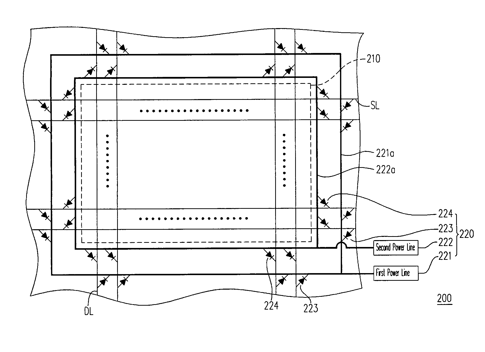
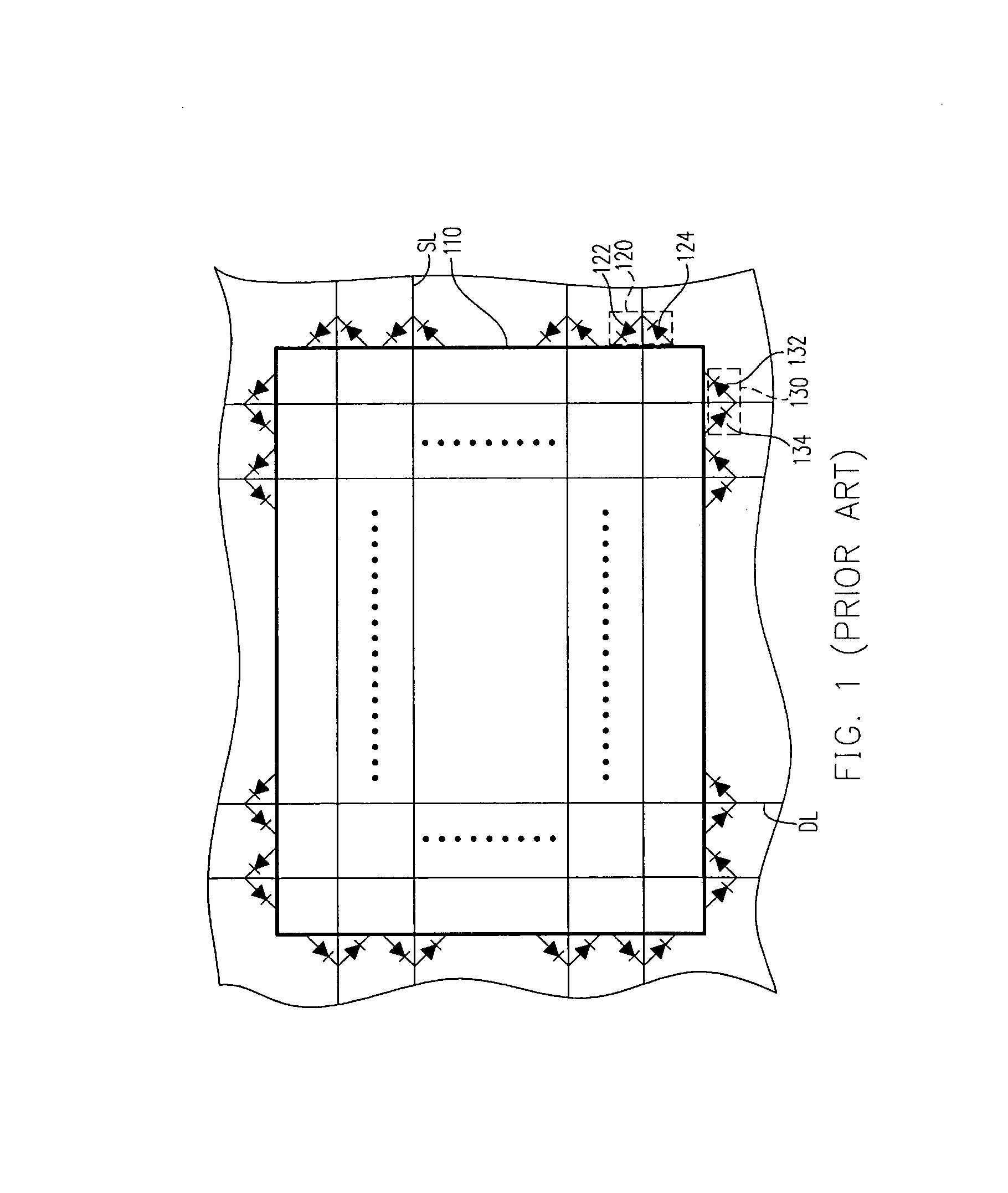
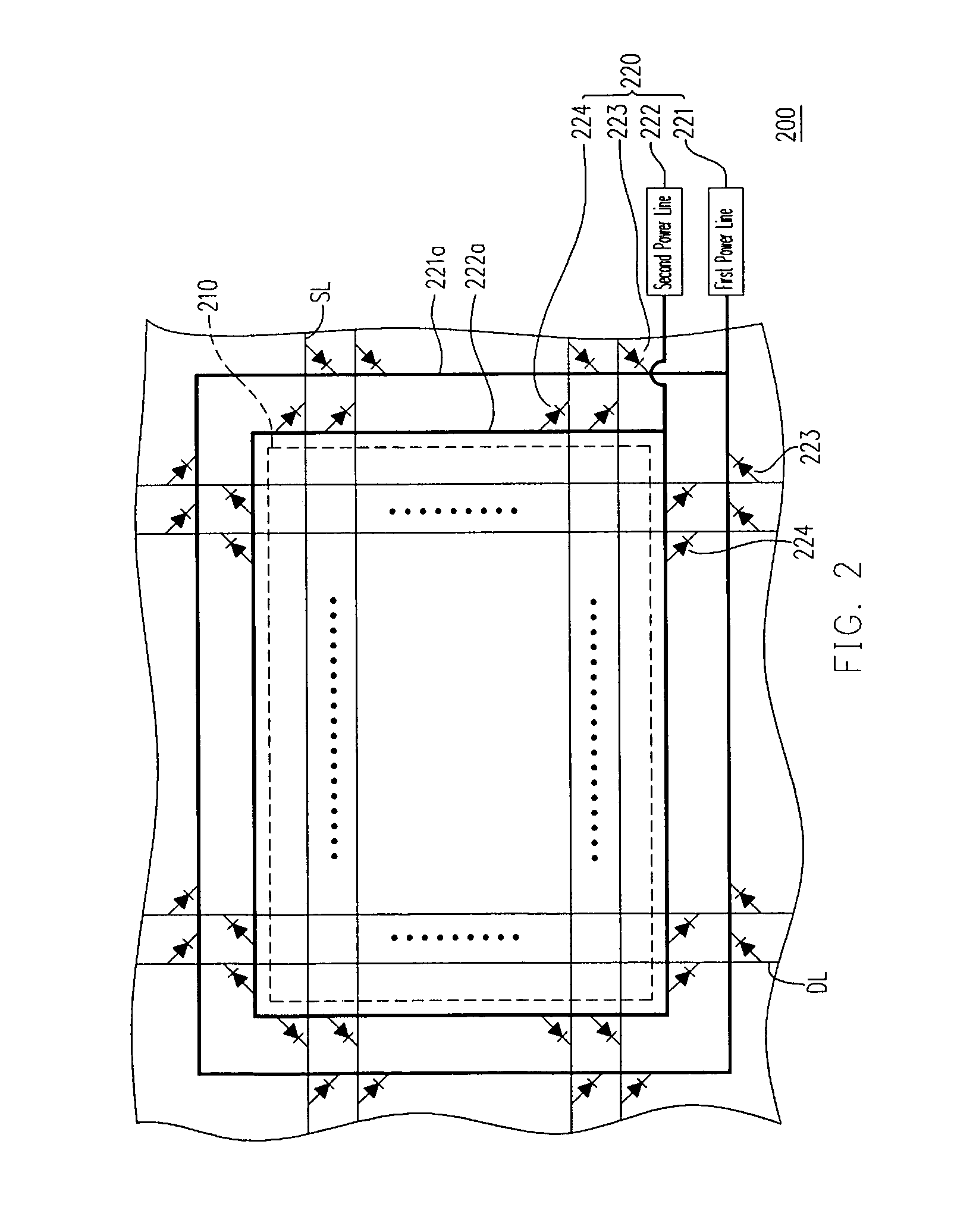
[0034]FIG. 2 is a schematic diagram showing an active matrix device having an ESD protection circuit according to a preferred embodiment of the present invention. Referring to FIG. 2, an active matrix device 200 comprises an active region 210 and an ESD protection circuit 220. The active region 210 comprises a plurality of scan lines SL and a plurality of data lines DL. A third voltage V3 and a fourth voltage V4 are the average voltages applied to the scan lines SL and the data lines DL respectively, to control the display status of each pixel. Generally speaking, the third voltage V3 is −15V, and the fourth voltage V4 is 2.5V. The ESD protection circuit 220 comprises a first power line 221, ...


PUM


Abstract

An active matrix device including an active region and an ESD protection circuit is provided. The active region includes scan lines and data lines. The ESD protection circuit includes a first power line, a second power line, a first diode and a second diode. The first diode is electrically connected between the scan line / data line and the first power line, and the second diode is electrically connected between the second power line and the scan line / data line. When a positive or negative ESD voltage is applied to the scan lines or the data lines, the ESD current is conducted to the first power line or the second power line through the first diodes or the second diodes, so as to protect the devices and circuits of the active matrix device from being damaged by the ESD zap.

Description

BACKGROUND OF THE INVENTION[0001]1. Field of the Invention[0002]The present invention generally relates to an active matrix device, and more particularly, to an active matrix device having an electrostatic discharge (ESD) protection design.[0003]2. Description of Related Art[0004]Electrostatic discharge is a phenomenon that occurs when static charges move on a non-conducting surface. The sudden movement of electric charges inside the semiconductor material of an integrated circuit (IC) package often leads to circuit failure. For example, people walking across a carpet may pick up static charges. If the relative humidity (RH) of the surrounding air is high, the human body may build up static charges that range up to thousands volts. However, if the RH of the surrounding air is low, the human body may build up static charges up to tens of thousands or more volts.[0005]Generally, during the fabrication process of an active matrix device, such as a liquid crystal display (LCD), an organ...

Claims


Application Information

Patent Timeline
IPC IPC(8): H02H9/00
CPCH01L23/60H01L27/0251H01L2924/12044H01L2924/0002H01L2924/00H01L27/04
Inventor HSU, YU-CHENLIU, CHUAN-FENGKUO, CHIA-HAO
Owner E INK HLDG INC
Features
  • R&D
  • Intellectual Property
  • Life Sciences
  • Materials
  • Tech Scout
  • Unparalleled Data Quality
  • Higher Quality Content
  • 60% Fewer Hallucinations
Learn More