Method for Pattern Formation Using Photoresist Cleaning Solution

a cleaning solution and photoresist technology, applied in the direction of photosensitive materials, instruments, photomechanical equipment, etc., can solve the problems of undesired pattern formation in the unexposed area, solubility differences between exposed and undesired patterns, and achieve the effect of preventing the diffusion of generated acid and avoiding undesired photoresist patterns

Inactive Publication Date: 2007-11-22
SK HYNIX INC
View PDF32 Cites 5 Cited by
  • Summary
  • Abstract
  • Description
  • Claims
  • Application Information

AI Technical Summary

Problems solved by technology

This alteration in polarity of the polymer matrix results in solubility differences between the exposed and the unexposed portions of the polymer in the developing solution.
However, the protecting group of the polymer compound in the photoresist can be detached during the baking step by small amounts of acid, so that the unexposed photoresist is dissolved in the developing solution and an undesired pattern is formed in the unexposed area.

Method used


Image

  • Method for Pattern Formation Using Photoresist Cleaning Solution
  • Method for Pattern Formation Using Photoresist Cleaning Solution
  • Method for Pattern Formation Using Photoresist Cleaning Solution

Examples


example 1

Preparation of Cleaning Solutions (1)

[0053] 0.1 g of polyethylene glycol having an average molecular weight of 4,600, and 1,000 g of H2O were mixed and stirred for 1 minute. The resulting mixture was filtered through 0.2 μm filter to obtain a cleaning solution composition of the present invention.

example 2

Preparation of Cleaning Solutions (2)

[0054] 0.1 g of polyethylene glycol monolaurate having an average molecular weight of 3,900, 30 g of ethanol and 970 g of H2O were mixed and stirred for 1 minute. The resulting mixture was filtered through 0.2 μm filter to obtain a cleaning solution composition of the present invention.

example 3

Formation of Photoresist Pattern (2)

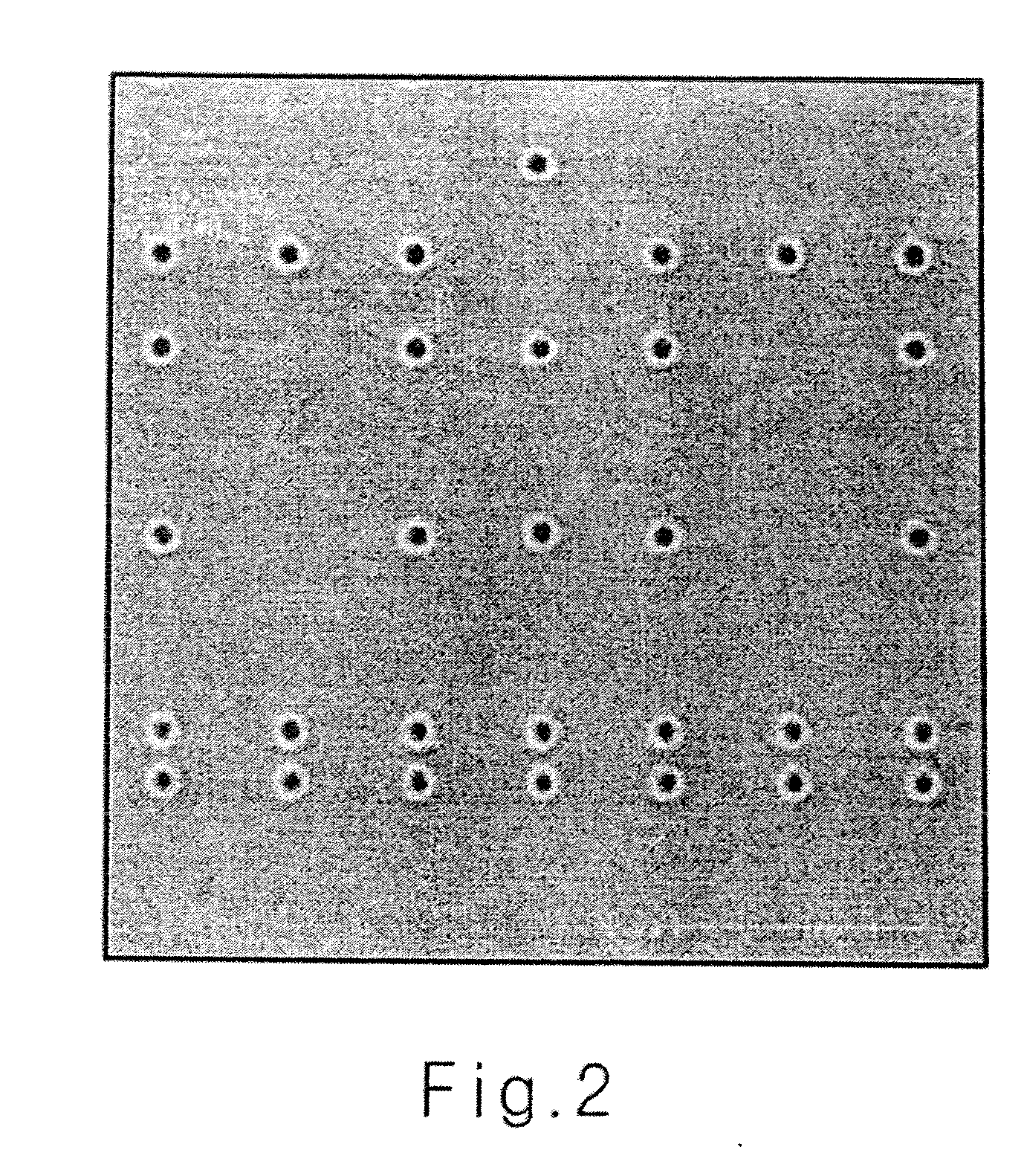
[0056] An underlying layer was formed on a silicon wafer treated with HMDS, and TarF-7a-39 product of TOK Co., Ltd., a methacrylate-type photosensitizer, was spin-coated on the surface of the underlying layer to form a photoresist film at thickness of 3,500 Å. Then, the photoresist film was soft-baked in an oven at 130° C. for 90 seconds. After soft-baking, the photoresist film was exposed to light using an ArF laser exposure device, and 100 mL of the cleaning solution composition obtained from Example 1 was sprayed on the photoresist film from upper portion of a spin device while the silicon wafer was spun on a spin device.

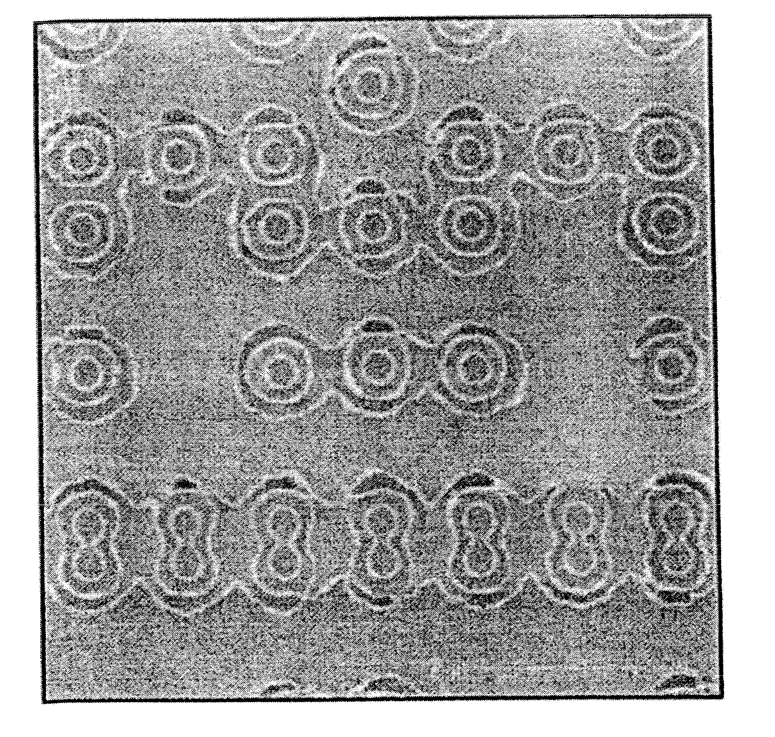
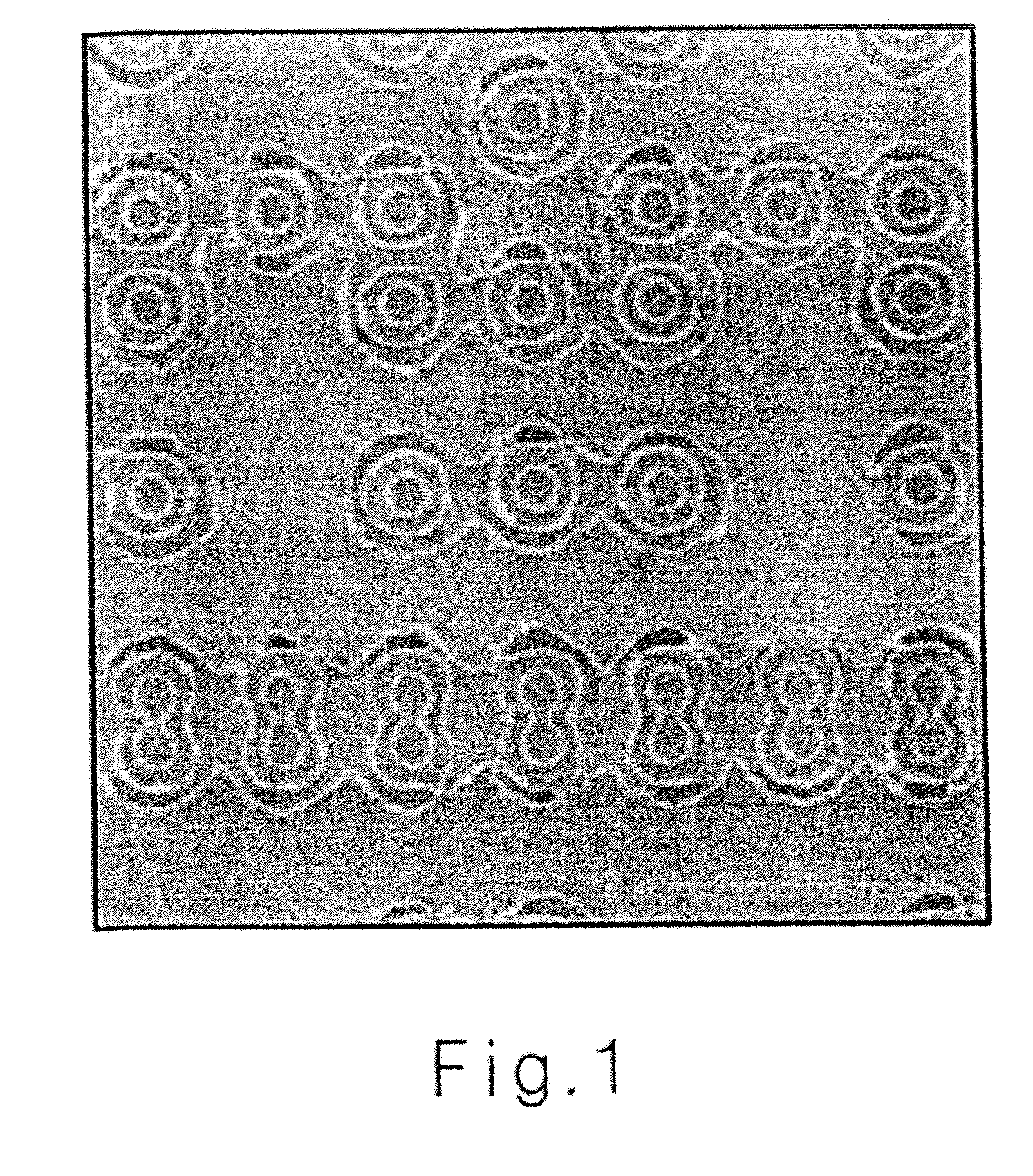
[0057] Then, the photoresist film was post-baked in the oven at 130° C. for 90 seconds, and then developed in a 2.38 wt. % aqueous TMAH solution for 30 seconds to obtain a 150 nm contact hole pattern (see FIG. 2). As a result, it was found that no pattern was formed in the undesired regions in comparison with FIG. 1.


PUM

PropertyMeasurementUnit
temperatureaaaaaaaaaa
total weightaaaaaaaaaa
polarityaaaaaaaaaa

Abstract

Photoresist cleaning solutions are used to clean semiconductor substrates before or after an exposing step when photoresist patterns are formed. The cleaning solutions include H2O and a nonionic surfactant compound represented by Formula 1. By spraying the disclosed cleaning solutions on a surface of the semiconductor substrate before or after exposing step to form a photoresist pattern, the desired pattern only is obtained and unnecessary patterns generated in undesired regions by ghost images are avoided as excess acid generated by the photoacid generator is neutralized and removed and damage to unexposed portions of the photoresist polymer is avoided. wherein R1 and R2 are independently H, C1-C20 alkyl, C5-C25 alkyl aryl or C1-C10 ester; m is 1 or 2; n is an integer ranging from 10 to 300; and o is 0 or 1.

Description

CROSS-REFERENCE TO RELATED APPLICATIONS [0001] This is a divisional of U.S. application Ser. No. 10 / 996,636 filed Nov. 23, 2004, which claims the priority benefit of KR 2003-84086 filed Nov. 29, 2003, the respective disclosure of which are incorporated herein by reference.BACKGROUND [0002] 1. Technical Field [0003] Photoresist cleaning solutions for rinsing semiconductor substrates before or after an exposing step during photoresist pattern formation are disclosed. More specifically, photoresist cleaning solutions are disclosed which comprise H2O and a nonionic surfactant compound as an additive. Methods for forming a photoresist pattern using the same are also disclosed. [0004] 2. Description of the Related Art [0005] Conventional methods for forming photoresist patterns on a semiconductor substrate comprise forming an underlying layer on a semiconductor substrate, forming a photoresist film on the underlying layer, and then exposing the photoresist film to light and developing the...

Claims


Application Information

Patent Timeline
Patent Type & Authority Applications(United States)
IPC IPC(8): G03C5/305G03F7/32G03C5/00G03F7/16G03F7/38
CPCG03F7/38G03F7/168G03F7/32
Inventor LEE, WON WOOKLEE, GEUN SUKIM, SAM YOUNG
Owner SK HYNIX INC
Why Eureka
Try Eureka